Semiconductor device capable of preventing erroneous operation attributed to electrostatic noise, and input device and scanner equipped therewith

a semiconductor and noise-related technology, applied in the direction of electronic switching, pulse technique, television system, etc., can solve the problems of incorrect data transfer to the subsequent ic, poor image quality, poor quality, etc., and achieve the effect of preventing an erroneous operation

Inactive Publication Date: 2006-10-12
ROHM CO LTD
View PDF13 Cites 5 Cited by
  • Summary
  • Abstract
  • Description
  • Claims
  • Application Information

AI Technical Summary

Benefits of technology

[0015] The present invention provides a semiconductor device that can eliminate the necessity of inserting an analog filter at clock signal line of a plurality of cascaded ICs to prevent an erroneous operation attributed to electrostatic noise, and an input device equipped therewith.

Problems solved by technology

The pulsed electrostatic noise causes an error in taking in data and the taken image may have a lateral line therein and hence poor quality.
However, external input signal SDI2 has transitioned low, and data will not be transferred to the subsequent IC correctly.
As such, if as shown in FIG. 12 static electricity is discharged or the like and accordingly a pulsed noise is input to the clock and data is taken in erroneously, the obtained image may have a lateral line therein resulting in poor image quality.
As a result, noise is readily introduced.
As such, it has been difficult to employ means preventing electrostatic noise.

Method used


Image

  • Semiconductor device capable of preventing erroneous operation attributed to electrostatic noise, and input device and scanner equipped therewith
  • Semiconductor device capable of preventing erroneous operation attributed to electrostatic noise, and input device and scanner equipped therewith
  • Semiconductor device capable of preventing erroneous operation attributed to electrostatic noise, and input device and scanner equipped therewith

Examples


first embodiment

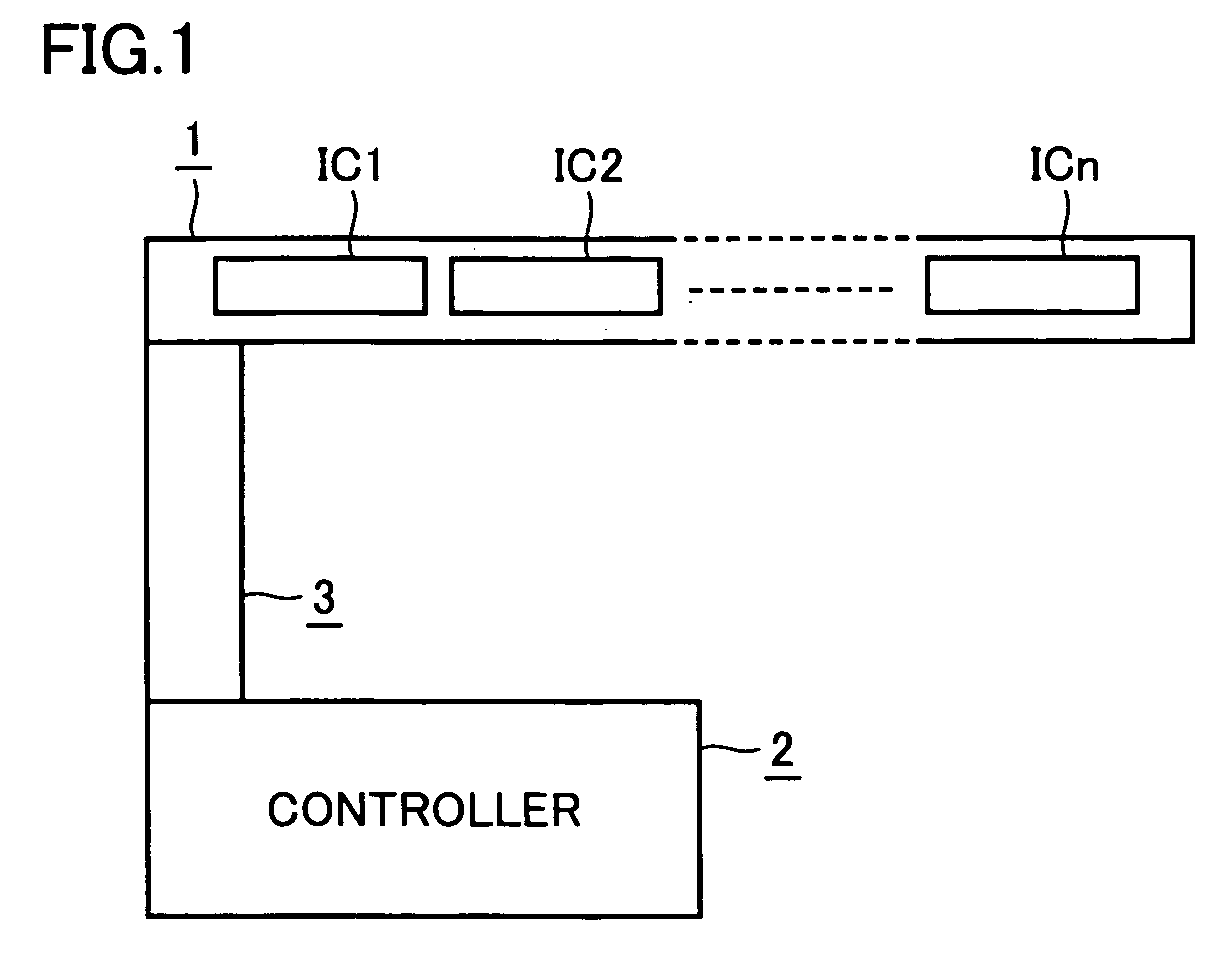
[0056]FIG. 1 shows a configuration of an input device in one embodiment having the present semiconductor device applied thereto.

[0057] With reference to FIG. 1, the present embodiment provides semiconductor devices IC1, IC2 . . . ICn disposed along a longer side of a rectangular input device 1 (corresponding in FIG. 9 to image sensor unit 91). Input device 1 is connected by a flexible cable 3 (corresponding in FIG. 9 to flexible cable 93) to a controller 2 (corresponding in FIG. 9 to controller 92). Note that through flexible cable 3 from input device 1 an input signal is input to controller 2, and from controller 2 through flexible cable 3 input device 1 receives a clock signal, a mode switching signal and other similar control signals.

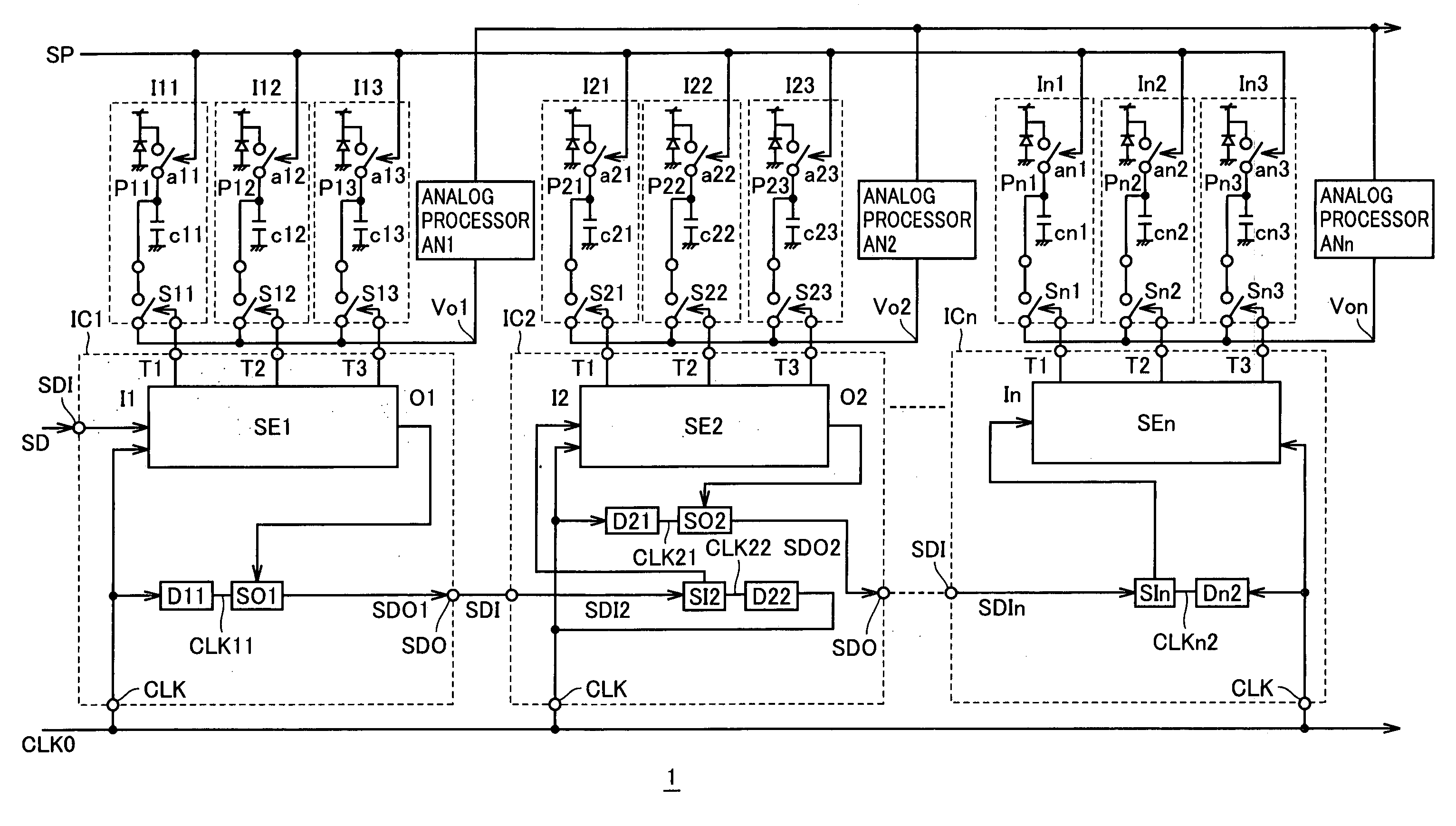
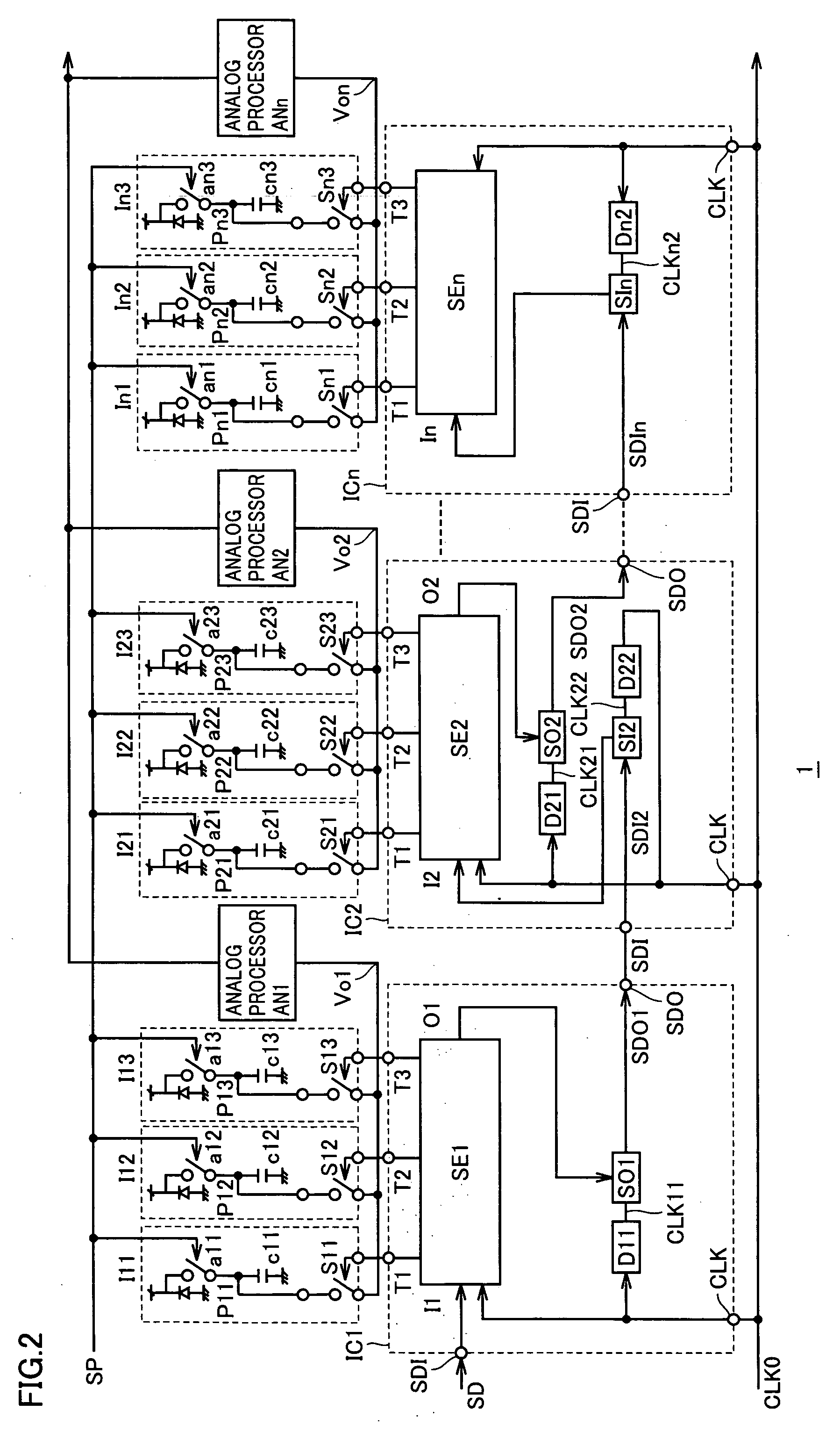
[0058]FIG. 2 shows a circuit configuration of input device 1.

[0059] With reference to FIG. 2, input device 1 has a plurality of semiconductor devices IC1, IC2, . . . , ICn with adjacent external control signal output and input terminals SDO and SD...


PUM


Abstract

A semiconductor device includes: a plurality of external signal input means; an external input unit having a switch each connected between the external signal input means and a read line and electrically connected for output from the external signal input means on the read line; a shift register receiving an external control signal and an external clock signal and synchronized with the external clock signal to shift successively the external control signal to provide shifted data and output the external control signal to electrically connect the switches in accordance with the shifted data; an output circuit receiving the external control signal from the shift register and externally outputting the external control signal; and a frequency divider circuit dividing the external clock signal in frequency to generate and output an internal clock signal, wherein the output circuit is synchronized with the internal clock signal to externally output the external control signal.

Description

BACKGROUND OF THE INVENTION [0001] 1. Field of the Invention [0002] The present invention relates generally to cascaded semiconductor devices, and particularly to semiconductor devices and input devices employing the same characterized in that adjacent integrated circuits (ICs) employ an internal clock obtained by processing a clock employed as a signal timing an external parallel input to enhance resistance to electrostatic noise and the like. [0003] 2. Description of the Background Art [0004] A scanner reading a variety of types of image data, for example as shown in FIG. 9, has a glass plate 94 securing an original thereon, and moves an image sensor unit 91 illuminating the original with light while reading an image. A flat bed scanner 9 includes an image sensor unit 91 reading an image, a controller 92 receiving a signal from image sensor unit 91 and processing and outputting the signal for example to a computer, a flexible cable 93 connecting controller 92 and image sensor unit...

Claims


Application Information

Patent Timeline
Patent Type & Authority Applications(United States)
IPC IPC(8): H03K17/00
CPCH04N1/193H04N1/1938H04N1/1934
Inventor YAMADA, NOBUYUKITAMAGAWA, TOSHIMITSU
Owner ROHM CO LTD
Why Eureka
Try Eureka