Bias circuit for high-swing cascode current mirrors

a bias circuit and cascode current mirror technology, applied in the field of electromechanical circuits, can solve the problems of not being able to tolerate as large of the output voltage swing, more voltage headroom to operate properly, and most cascode current mirrors are not suitable for use in a low-voltage power supply environmen

Inactive Publication Date: 2006-10-12
AVAGO TECH INT SALES PTE LTD
View PDF9 Cites 22 Cited by
  • Summary
  • Abstract
  • Description
  • Claims
  • Application Information

AI Technical Summary

Benefits of technology

[0005] The present invention meets the above-noted need by providing, in an illustrative embodiment, an impr...

Problems solved by technology

Unfortunately, however, cascode current mirrors typically require more voltage headroom to operate properly, and therefore cannot tolerate as large of an output voltage swing as can be tolerated by simple current mirror arrangements.
Consequently, most cascode current mirrors are not suitable for use in a low-voltage pow...

Method used


Image

  • Bias circuit for high-swing cascode current mirrors
  • Bias circuit for high-swing cascode current mirrors
  • Bias circuit for high-swing cascode current mirrors

Examples


Embodiment Construction

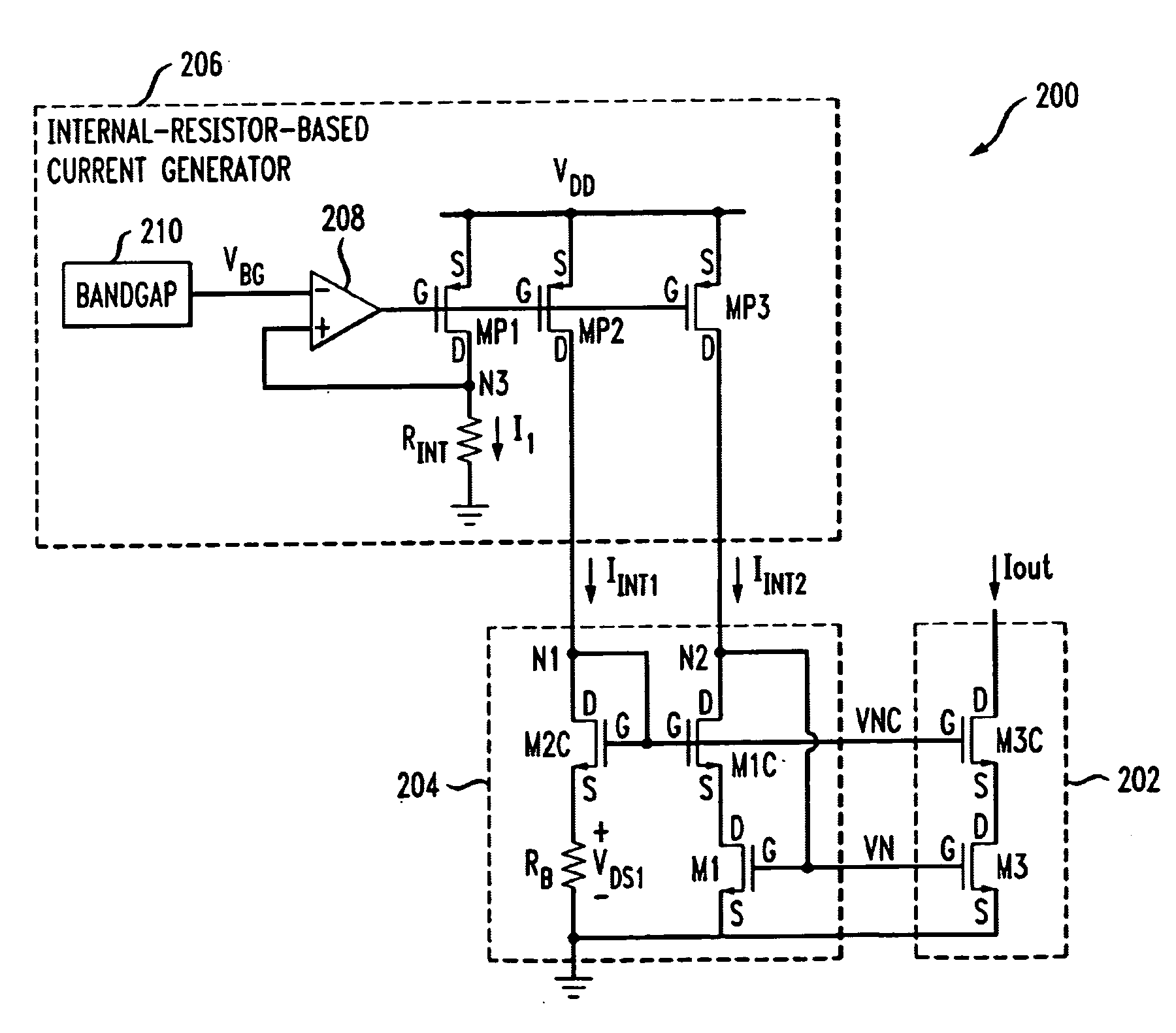
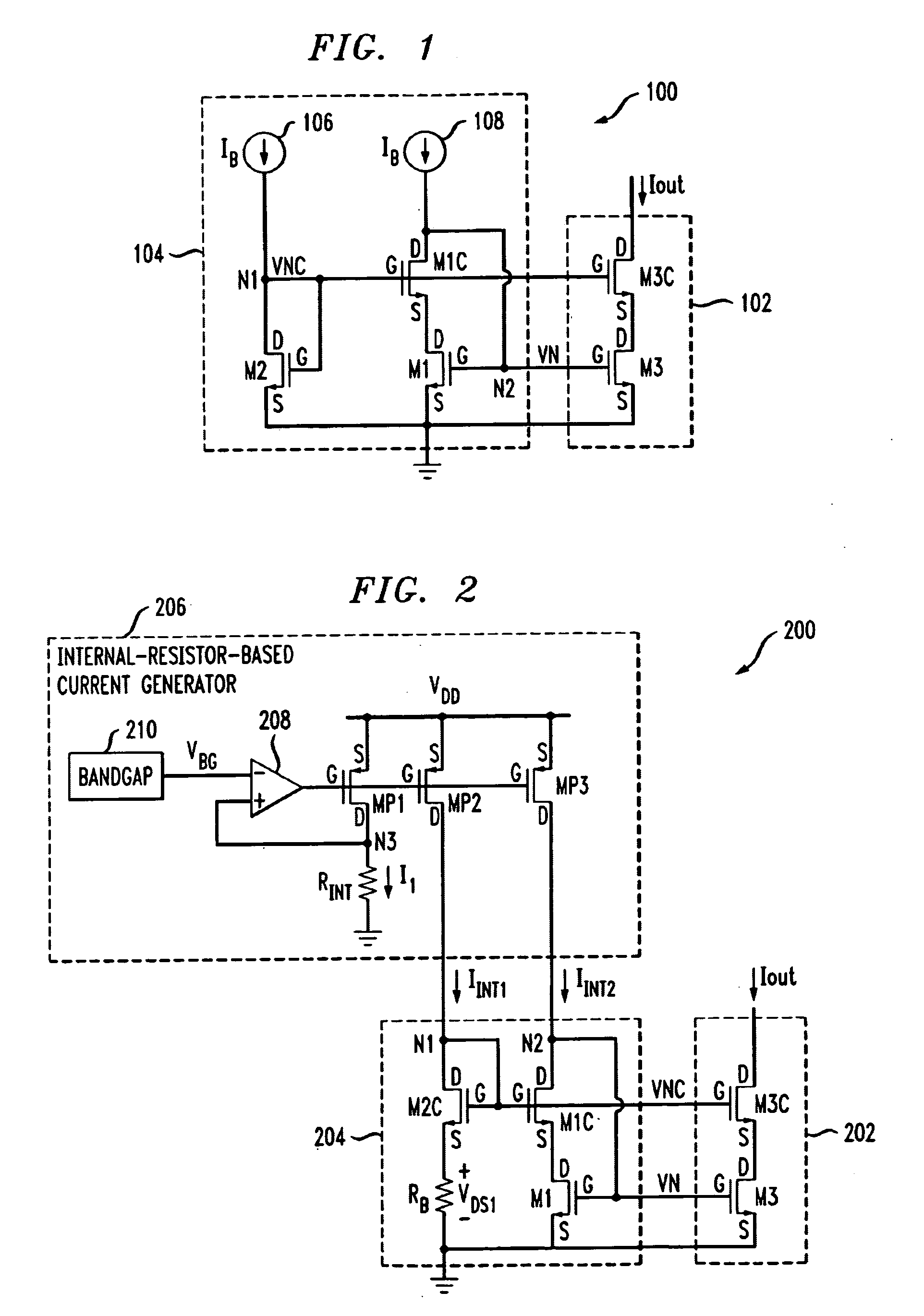
[0013] The present invention will be described herein in the context of illustrative bias circuits. It should be understood, however, that the present invention is not limited to these or any particular circuit arrangements. Rather, the invention is more generally applicable to techniques for generating cascode bias voltages for biasing high-swing cascode current sources and / or current sinks. Although implementations of the present invention are described herein with specific reference to p-channel metal-oxide-semiconductor (PMOS) and n-channel metal-oxide-semiconductor (NMOS) transistor devices, as may be formed using a complementary metal-oxide-semiconductor (CMOS) fabrication process, it is to be understood that the invention is not limited to such transistor devices and / or such a fabrication process, and that other suitable devices, such as, for example, bipolar junction transistors (BJTs), etc., and / or fabrication processes (e.g., bipolar, BiCMOS, etc.), may be similarly employ...


PUM


Abstract

A bias circuit for providing at least first and second bias signals for biasing a cascode current source and/or a cascode current sink includes a resistive element and first, second and third transistors, each transistor having first and second source/drain terminals and a gate terminal. The first source/drain terminal of the first transistor is coupled to the gate terminal, the first bias signal being generated at the first source/drain terminal in response to receiving a first reference current at the first source/drain terminal. A first end of the first resistive element is coupled to the second source/drain terminal of the first transistor. The gate terminal of the second transistor is coupled to the gate terminal of the first transistor, the second bias signal being generated at the first source/drain terminal of the second transistor in response to receiving a second reference current at the first source/drain terminal of the second transistor. The first source/drain terminal of the third transistor is coupled to the second source/drain terminal of the second transistor, the second source/drain terminal of the third transistor is coupled to a second end of the first resistive element, and the gate terminal of the third transistor is coupled to the first source/drain terminal of the second transistor.

Description

FIELD OF THE INVENTION [0001] The present invention relates generally to electronic circuits, and more particularly relates to improved bias circuits suitable for biasing high-swing cascode current sources and / or current sinks. BACKGROUND OF THE INVENTION [0002] Current mirrors, which are used primarily as a means for replicating a reference current, are employed in a variety of analog circuits, such as, but not limited to, reference generators, amplifiers, and digital-to-analog converters. A current mirror is designed to receive a reference current and to generate an output current which is identical to, or proportional to, the reference current at an output of the current mirror. A current mirror typically includes a current source and / or a current sink, and a bias circuit for biasing the current source and / or current sink. An ideal current mirror may be characterized as having essentially an infinite parallel output impedance, such that its output current is independent of the vo...

Claims


Application Information

Patent Timeline
IPC IPC(8): G05F1/10
CPCG05F3/262
Inventor ABEL, CHRISTOPHER J.
Owner AVAGO TECH INT SALES PTE LTD
Why Eureka
Try Eureka