High-density low-power data retention power gating with double-gate devices

Active Publication Date: 2006-10-19
GLOBALFOUNDRIES US INC
View PDF10 Cites 32 Cited by
  • Summary
  • Abstract
  • Description
  • Claims
  • Application Information

AI Technical Summary

Benefits of technology

[0006] Generally, in accordance with at least one presently preferred embodiment of the present invention, there is broadly contemplated herein a novel power-gating structure using a single DG device to provide both power switch and virtu

Problems solved by technology

It is generally known that the leakage power consumption of VLSI logic and memories increases rapidly with CMOS technology scaling.
However, such a power gating structure (FIG. 1(a)) is not widely used in latches and other memory elements since the stored data information

Method used


Image

  • High-density low-power data retention power gating with double-gate devices
  • High-density low-power data retention power gating with double-gate devices
  • High-density low-power data retention power gating with double-gate devices

Examples


Embodiment Construction

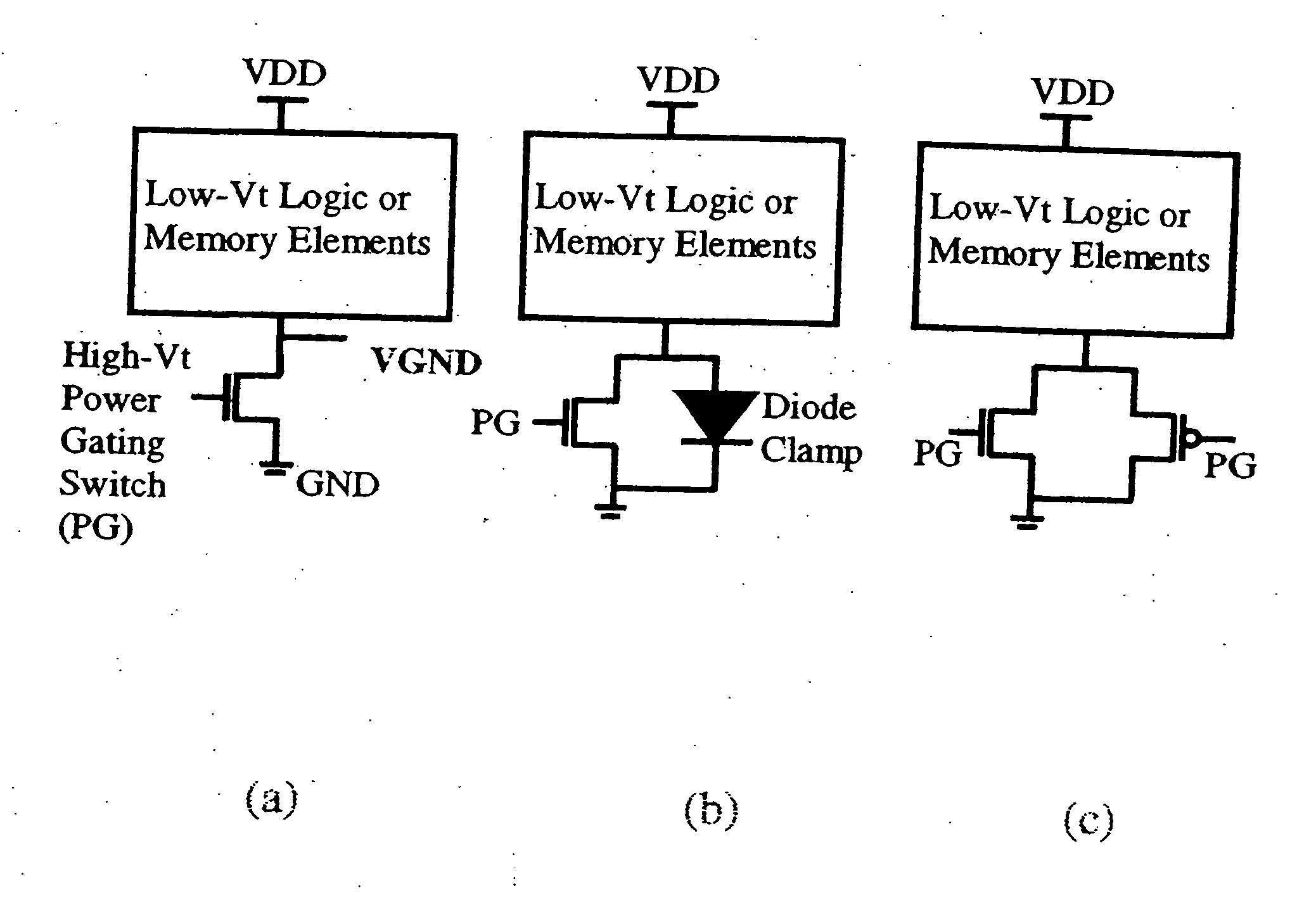
[0023] As mentioned above, FIGS. 1(a), (b), and (c) show conventional (footer-based) power gating structures. In the most primitive form (FIG. 1(a)), the power line is cut off by an nFET power switch. The virtual ground (VGND) is left floating when the power switch device is off during the sleep / standby mode. As the virtual ground is charged up by the leakage, it gradually drifts to higher voltage, thus squeezing the voltage across memory elements and resulting in lost of stored data. By putting an extra diode (FIG. 1(b)) or a pFET (FIG. 1(c)) as clamping device, the voltage level of virtual GND is prevented from rising too high and adequate voltage is maintained across the memory elements. However, in addition to the extra leakage current path through the clamping device, the area and capacitance of the power gating structure are increased, thereby degrading the performance and power. Furthermore, for power gating structures with complementary CMOS devices (FIG. 1(c)), additional t...


PUM


Abstract

A new power gating structure with robust data retention capability using only one single double-gate device to provide both power gating switch and virtual supply/ground diode clamp functions. The scheme reduces the transistor count, area, and capacitance of the power gating structure, thus improving circuit performance, power, and leakage. The scheme is compared with the conventional power gating structure via mixed-mode physics-based two-dimensional numerical simulations. Analysis of virtual supply/ground bounce for the proposed scheme is also presented.

Description

[0001] This invention was made Government support under Contract No. NBCH3039004 awarded by DARPA. The Government has certain rights in this invention.FIELD OF THE INVENTION [0002] The present invention generally relates to a method for data generation with systematic modelling. BACKGROUND OF THE INVENTION [0003] Numerals presented herebelow in square brackets -[ ]- are keyed to the list of references found towards the close of the present disclosure. [0004] Initial reference is made to FIGS. 1(a), (b) and (c). It is generally known that the leakage power consumption of VLSI logic and memories increases rapidly with CMOS technology scaling. One way to reduce the power is to cut off the power line in standby mode when the circuit is not operating [1]. However, such a power gating structure (FIG. 1(a)) is not widely used in latches and other memory elements since the stored data information is completely lost when the power switch is off, and data recovery process significantly degrad...

Claims


Application Information

Patent Timeline
IPC IPC(8): H03K17/687
CPCH01L27/105H01L27/11H01L27/1116G11C5/14H01L29/78648H03K3/356156H01L29/785H10B10/18H10B10/00
Inventor CHUANG, CHING-TE K.DAS, KOUSHIK K.KIM, KEUNWOO
Owner GLOBALFOUNDRIES US INC
Why Eureka
Try Eureka