Device and method for transmitting data in an encrypted manner

a technology of encryption and data transmission, applied in the field of cryptography, can solve the problems of additional safety risks, difficult to achieve the processing speed of such complex algorithms on the individual semiconductor chip, and the need for safety measures against new attack scenarios

Active Publication Date: 2006-10-19
INFINEON TECH AG
View PDF4 Cites 13 Cited by
  • Summary
  • Abstract
  • Description
  • Claims
  • Application Information

AI Technical Summary

Problems solved by technology

Due to the clear increase in complexity in modern algorithms or circuits, the area available on a single semiconductor chip frequently is no longer sufficient to guarantee a compact integrated circuit and thus, by a small line length in this circuit, fast processing of such complex algorithms on the individual semiconductor chip is difficult to achieve.
However, such a partitioning of the processing of an algorithm or partitioning of a corresponding safety controller into two chips entails, additional safety risks and requires safety measures against new attack scenarios.

Method used


Image

  • Device and method for transmitting data in an encrypted manner
  • Device and method for transmitting data in an encrypted manner

Examples


Embodiment Construction

[0030] In the Figures, same or similar elements are characterized by same or similar reference numerals, a repeated description of these reference numerals being omitted.

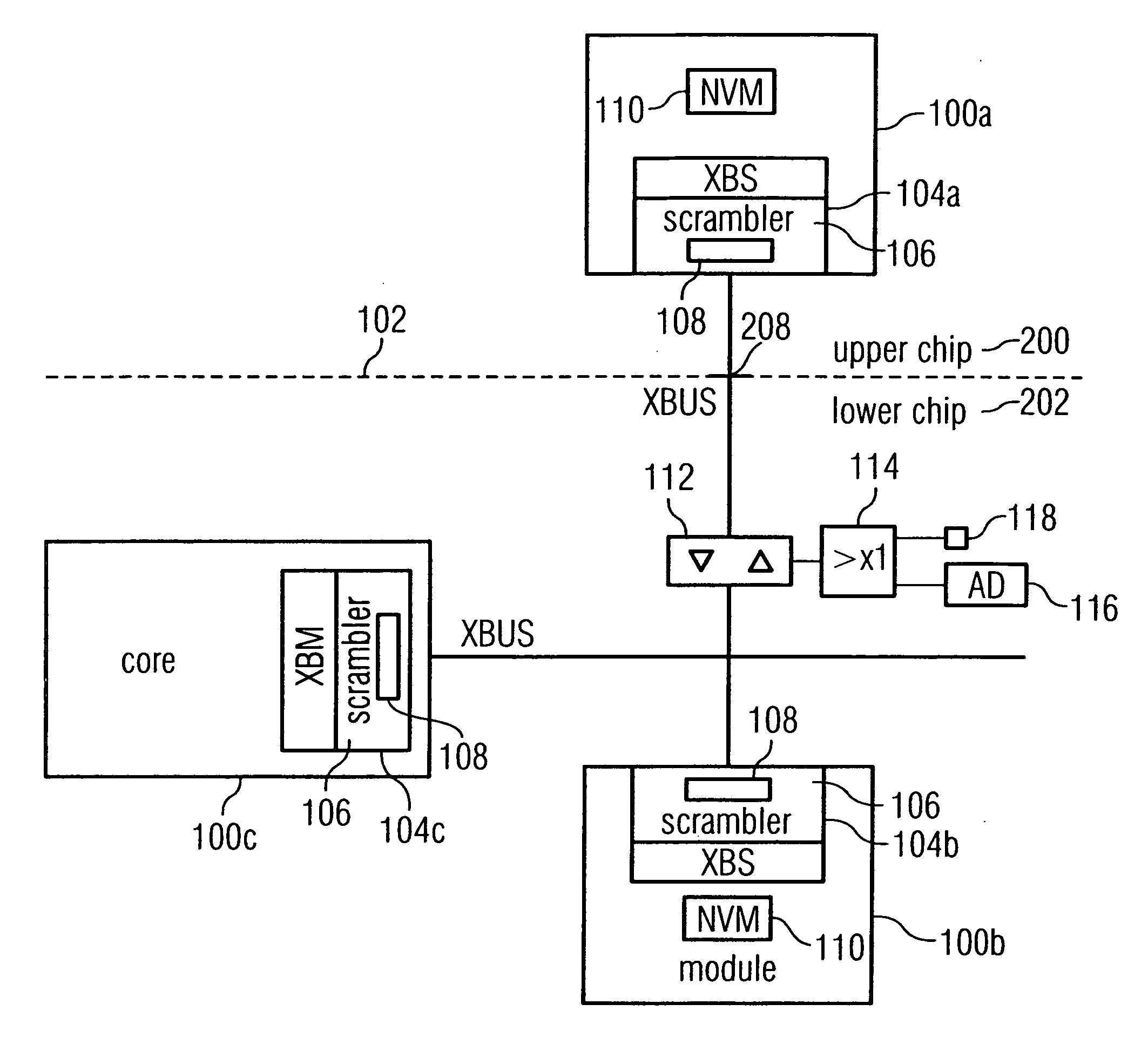
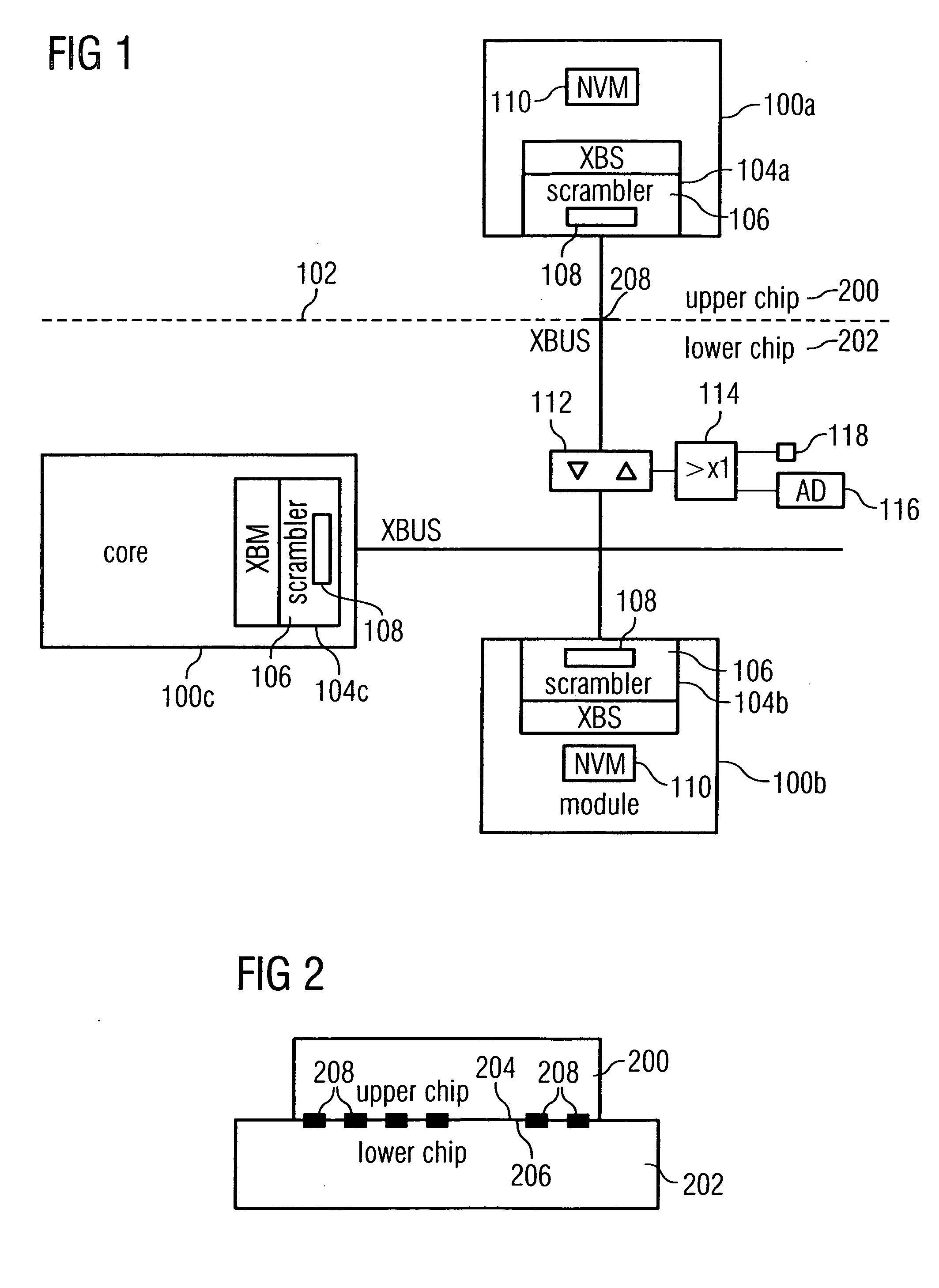
[0031]FIG. 1 shows a block circuit diagram of an embodiment of a device according to the present invention. The device illustrated in FIG. 1 includes several functional blocks 100a to 100c which can be disposed in different semiconductor chips. The broken line 102 in FIG. 1 characterizes a partitioning of the association of the functional block 100a to 100c on the upper chip and the lower chip so that the functional block 100a according to FIG. 1 is disposed in the upper chip (i.e. exemplarily in the chip 200 illustrated in FIG. 2) and the functional blocks 100b and 100c are disposed in the lower chip (i.e. in the lower chip 202 in FIG. 2). Each of the three functional units 100a to 100c includes a data transmission interface 104a to 104c, each including a scrambler 106 having a stream encryption unit 108. In addit...


PUM


Abstract

A device according to the present invention is configured for transmitting data between two semiconductor chips of a data processor in an encrypted manner, wherein a first semiconductor chip is connected to a second semiconductor chip. The device includes a non-volatile memory element in each of the two semiconductor chips, wherein an encryption initial value for an encryption rule is stored in the memory element of the first semiconductor chip and a decryption initial value associated to the encryption initial value for a decryption rule associated to the encryption rule is stored in the memory element of the second semiconductor chip. Additionally, the first semiconductor chip has a first data transmission interface formed to generate an encryption data stream from an input data stream using the encryption initial value according to the encryption rule. Also, the second semiconductor chip has a second data transmission interface formed to receive the encryption data stream and to generate a decryption data stream from the encryption data stream using the decryption initial value according to the decryption rule and to compare the decryption data stream generated to an expected data stream, wherein the second data transmission interface is also formed to perform a defensive measure against transmitting data from the second data transmission interface to the first data transmission interface when the decryption data stream does not correspond to the expected data stream.

Description

BACKGROUND OF THE INVENTION CROSS-REFERENCE TO RELATED APPLICATION [0001] This application claims priority from German Patent Application No. 10 2005 013 830.6, which was filed on Mar. 24, 2005, and is incorporated herein by reference in its entirety. [0002] 1. Field of the Invention [0003] The present invention relates to the technical field of cryptography and, in particular, the present invention relates to the technical sub-field of the cryptographic protection of a data exchange of two semiconductor chips. [0004] 2. Description of Related Art [0005] Due to the clear increase in complexity in modern algorithms or circuits, the area available on a single semiconductor chip frequently is no longer sufficient to guarantee a compact integrated circuit and thus, by a small line length in this circuit, fast processing of such complex algorithms on the individual semiconductor chip is difficult to achieve. In order to counter this problem, two chips are frequently connected to each oth...

Claims


Application Information

Patent Timeline
Patent Type & Authority Applications(United States)
IPC IPC(8): H04K1/06H04L9/00H04K1/04
CPCG06F21/85H04L2209/34H04L2209/12H04L9/065
Inventor GAMMEL, BERNDTSCHEIBLHOFER, DIETMAR
Owner INFINEON TECH AG
Why Eureka
Try Eureka