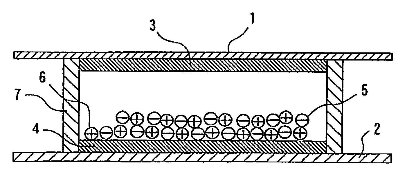
Image display unit

a display unit and image technology, applied in static indicating devices, non-linear optics, instruments, etc., can solve the problems of slow response speed, lack of imaging repetition stability, difficult to maintain a stable dispersion state, etc., to achieve excellent stability, simple and inexpensive construction, and rapid response speed

Inactive Publication Date: 2006-10-26
BRIDGESTONE CORP
View PDF2 Cites 112 Cited by
  • Summary
  • Abstract
  • Description
  • Claims
  • Application Information

AI Technical Summary

Benefits of technology

[0014] An object of the first aspect of the invention is to provide an image display device of dry type having rapid response, simple and inexpensive construction, and excellent stability, which can reduce density unevenness and maintain a display quality.
[0015] According to the first aspect of the invention, an image display device which comprises an image display panel, in which two or more groups of particles having different colors and different charge characteristics are sealed between two substrates, at least one of two substrates being transparent, and, in which the particles, to which an electrostatic field produced by a pair of electrodes provided on one or both substrates is applied, are made to fly and move so as to display an image, is characterized in that the image display device has an image (to be displayed) forming process comprising an image forming process for forming the image by applying an electric field pattern between the electrodes, the electric field pattern serving to fly particles A to the substrate at an image display side; and an image forming process for forming the image by applying an inversion (negative) electric field pattern with respect to the electric field pattern, the inversion electric field pattern serving to fly particles B having different colors and different charge characteristics with respect to those of the particles A to the substrate at an image display side; so that an image deleting process prior to forming the image to be displayed is eliminated.
[0016] According to the image display device of the first aspect of the invention, since a novel image display device is constructed by arranging image display elements in a matrix manner, which can fly and move the particles by means of Coulomb's force and so on when an electrostatic field is directly applied to the particles, it is possible to obtain an image display device which can realize rapid response, simple and inexpensive construction, and excellent stability. Moreover, since the image deleting process prior to forming the image to be displayed is eliminated, it is possible to reduce density unevenness and maintain the display quality.

Problems solved by technology

However, in the electrophoresis method, there is a problem that a response speed is slow by the reason of viscosity resistance because the particles migrate among the electrophoresis solution.
Further, there is a problem of lacking imaging repetition stability, because particles with high specific gravity of titanium oxide is scattered within solution of low specific gravity, it is easy to subside, difficult to maintain a stability of dispersion state.
Even in the case of microencapsulating, cell size is diminished to a microcapsule level in order to make it hard to appear, however, an essential problem was not overcome at all.
However, the structure becomes complicated because the charge transport layer and further a charge generation layer are to be arranged.
In addition, it is difficult to constantly dissipate charges from the electro-conductive particles, and thus there is a drawback on the lack of stability.
Therefore, there is a drawback such that density unevenness occurs in the image and a display quality is extremely deteriorated.
However, the halftone image display according to the method mentioned above has a drawback such that the image memory property cannot be obtained.
However, the halftone image display according to the method mentioned above has a drawback such that a driving circuit of image display elements becomes complicated.
However, the halftone image display according to the method mentioned above has a drawback such that an excellent reproducibility of the halftone image display cannot be performed since resistivity and so on of ITO transparent electrode is deviated, an electrode surface is contaminated by a particle component, and a threshold voltage when the particles are moved from the electrode surface due to a throw off force larger than an adhesion force.
Therefore, especially in the case of performing the matrix drive that needs a precipitous threshold, the number of gray scales that can be displayed is limited.

Method used


Image

  • Image display unit
  • Image display unit
  • Image display unit

Examples


embodiment 1

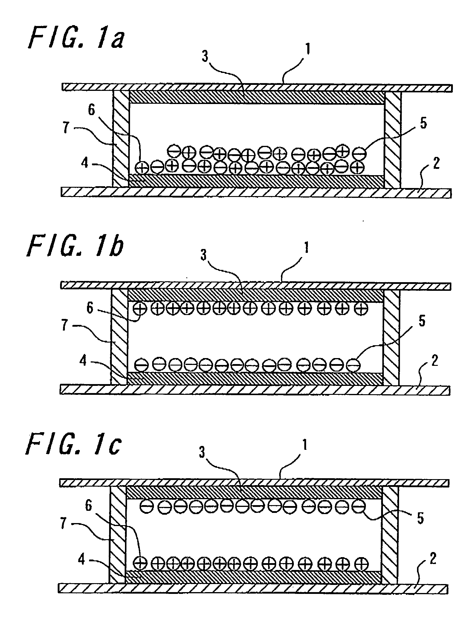
[0101] Hereinafter, a weiting means without using an image deleting process, which is a feature of the first aspect of the image display device according to the invention, will be explained with reference to drawings. In the examples shown in FIGS. 6 and 7, a rewriting operation from numeral “1” to numeral “2” is explained on the 7 lines×5 rows matrix display.

[0102] In the example shown in FIG. 6, the image is formed by switching a direction of the electric field to be applied sequentially during an image forming process of a portion where the display is rewritable at once (normally one line) on the 7 lines×5 rows matrix display. Specifically, if patterns of 1 . . . n lines of the image “2” to be written next are assumed as P1 . . . Pn, in order to switch the direction of the electric field at every one line, firstly the pattern P1 is written by Ea on the first line and then the pattern Not(P1) is written by Eb on the first line. Secondary, the pattern P2 is written by Ea on the se...

embodiment 2

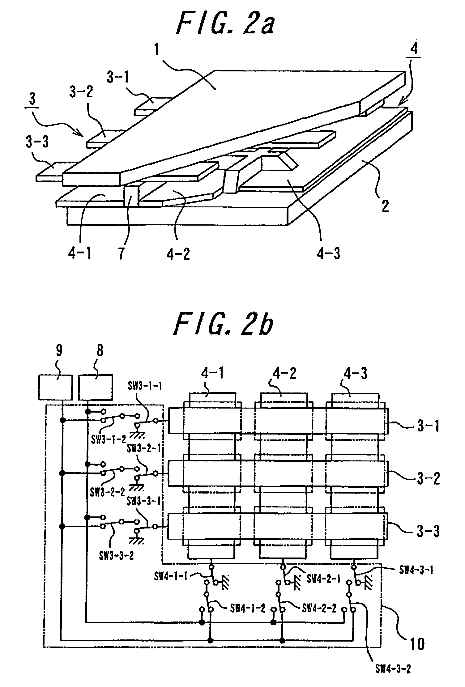
[0106] Then, the operation for the halftone image display (gray level display) and the particle sate reset operation prior to the halftone image display, which are performed by the second aspect of the image display device according to the invention, will be explained with reference to FIGS. 8a, 8b and FIG. 9.

[0107]FIG. 8a is a schematic view for explaining a method of applying a reset voltage for a particle state reset operation prior to a halftone image display in the image display device according to the second aspect of the invention, and FIG. 8b is a schematic view for explaining a method of applying an electric field for a halftone image display in the image display device according to the second aspect of the invention. In FIGS. 8a and 8b, a horizontally arranged rectangle corresponds to the display electrode 3, a vertically arranged rectangle corresponds to the opposed electrode 4, and an intersecting portion between the horizontally arranged rectangle and the vertically ar...

embodiment 3

[0114]FIGS. 10a to 10d are schematic views respectively showing one embodiment of sub-pixels in the third aspect of the image display device according to the invention. The embodiment shown in FIGS. 10a to 10d shows the sub-pixels obtained by segmentalizing one pixel unevenly. Specifically, one pixel (FIG. 10b) in the 20×20 dots matrix display shown in FIG. 10a is segmentalized into sub-pixels each having a different size. In this case, sizes of the sub-pixels are to be two's power i.e. six sub-pixels have sizes of 20(=1), 21(=2), 22(=4), 23(=8), 24(=16) and 25(=32) respectively.

[0115] As for a method of segmentalizing one pixel unevenly, as shown in FIG. 10c, use may be made of six sub-pixels each having a rectangular shape with a different area. Moreover, as shown in FIG. 10d, use may be made of six sub-pixels each having same width along a line direction and different width along a row direction, i.e. each having a different area. The uneven segmentalization shown in FIG. 10c is...


PUM

PropertyMeasurementUnit
particle diameteraaaaaaaaaa
thicknessaaaaaaaaaa
thicknessaaaaaaaaaa

Abstract

Each embodiment relates to an image display device which comprises an image display panel, in which two or more groups of particles having different colors and different charge characteristics are sealed between two substrates, at least one of two substrates being transparent, and, in which the particles, to which an electrostatic field produced by a pair of electrodes provided on one or both substrates is applied, are made to fly and move so as to display an image. Among them, in the first aspect of the invention, an image forming process for forming the image by applying an electric field pattern between the electrodes, the electric field pattern serving to fly particles A to the substrate at an image display side; and an image forming process for forming the image by applying an inversion (negative) electric field pattern with respect to the electric field pattern, the inversion electric field pattern serving to fly particles B having different colors and different charge characteristics with respect to those of the particles A to the substrate at an image display side; so that an image deleting process prior to forming the image to be displayed is eliminated.

Description

TECHNICAL FIELD [0001] The present invention relates to an image display device comprising an image display panel enables to repeatedly display or eliminate images accompanied by flight and movement of particles utilizing Coulomb's force and so on. BACKGROUND ART [0002] As an image display device substitutable for liquid crystal display (LCD), image display devices with the use of technology such as an electrophoresis method, an electro-chromic method, a thermal method, dichroic-particles-rotary method are proposed. [0003] As for these image display device, it is conceivable as inexpensive visual display device of the next generation from a merit having wide field of vision close to normal printed matter, having smaller consumption with LCD, spreading out to a display for portable device, and an electronic paper is expected. Recently, electrophoresis method is proposed that microencapsulate dispersion liquid made up with dispersion particles and coloration solution and dispose the l...

Claims


Application Information

Patent Timeline
Patent Type & Authority Applications(United States)
IPC IPC(8): G09G3/34G02F1/167G09G3/20
CPCG02F1/167G09G2320/0276G09G3/2011G09G3/2014G09G3/2022G09G3/2074G09G3/2077G09G3/2081G09G3/344G09G2300/0443G09G2300/06G09G2310/0251G09G2310/0275G09G2310/061G09G2310/068G09G2320/0233G09G2320/0261G02F2001/1674G02F1/1671
Inventor NIHEI, NORIOKITANO, HAJIMEYAKUSHIJI, GAKUMURATA, KAZUYATAKAGI, KOJIMASUDA, YOSHITOMOKAWAGOE, TAKAHIROHATTORI
Owner BRIDGESTONE CORP
Why Eureka
Try Eureka