Microwell arrays with nanoholes

a nano-hole and microwell technology, applied in the field of microwell arrays with nano-holes, can solve the problems of inconvenient and bulky implementation into parallel analysis automated systems, insufficient chemically sensitive or physically capable of obtaining single cell measurements, etc., and achieves low noise electrical measurements, high-resolution delivery, and high precision.

Inactive Publication Date: 2006-10-26
UNIV OF WASHINGTON
View PDF11 Cites 43 Cited by
  • Summary
  • Abstract
  • Description
  • Claims
  • Application Information

AI Technical Summary

Benefits of technology

[0005] The lab-on-a-chip device described here is a new generation cell culture tool that allows the interrogation of large number of single cells simultaneously. The device enables parallel electrophysiological measurements, such as measuring ion currents through ion channels residing in the plasma membrane, as well as delivery of key biochemical factors to multiple cells with a very high precision. To achieve this, an array of very small holes is created on a thin transparent membrane of silicon nitride or silicon oxide that is suspended on an array of wells through a silicon wafer. A microfluidic channel network, made of poly(dimethylsiloxane) or another appropriate polymer, on the membrane side of the wafer allows individual addressing of the holes. Because the holes provide the sole fluidic and electrical connection between the microfluidic network on one side and the wells on the other side, very low-noise electrical measurements and well-controlled high-resolution delivery of biomolecules to cells can be achieved. Individual cells are cultured inside each well on top of or a certain distance away from the hole, depending on the application. The cells can also be cultured on the membrane side of the device, and the fluidic delivery can be done from the well-side. In addition, both sides of the device can be separately addressed via microfluidic channels. The device is useful for a number of other applications, such as high-throughput screening for drug discovery, immunoisolation of cells, cell filtration and separation, biomolecular separation, and protein and DNA sequencing.

Problems solved by technology

One of the biggest challenges in cell biology, as well as in neuroscience, is being able to do parallel analysis on multiple individual cells.
This stems from the fact that most of the current cellular analysis tools and methods are not chemically sensitive enough for or physically capable of obtaining measurements from single cells.
They also are not suitable (e.g. too bulky) to be implemented into automated systems for parallel analysis and require relatively extensive human labor.

Method used


Image

  • Microwell arrays with nanoholes
  • Microwell arrays with nanoholes
  • Microwell arrays with nanoholes

Examples


example 1

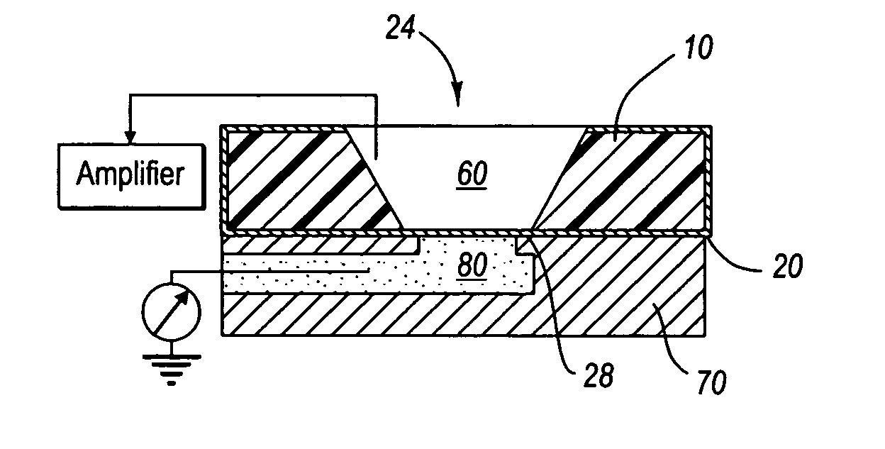
[0089]FIG. 15A is a cross-sectional view of a device comprising a silicon wafer 10 defining a microwell 60. A PDMS layer 70 with a microchannel 80 is positioned with the microchannel aligned with a microwell 60. Membrane layer 20 does not have a nanohole below microwell 60. FIG. 15B is a top view of the device shown in FIG. 15A. Test experiments were conducted using this device to determine whether it provides results comparable to a traditional patch-clamp set-ups. The microwells and microchannels were filled with electrolyte fluid. A square-wave voltage pulse was applied between microwell and the microchannel. Electrical resistance and capacitance were measured. The results of the experiments are shown in FIG. 15C. In the absence of a nanohole the current did not flow, showing that the suspended silicon nitride layer provides a good insulation.

example 2

[0090]FIG. 16A is a cross-sectional view of a device similar to the device described in connection with FIGS. 15A-15B except that membrane 20 defines a 1 μm nanohole 22 between microwell 60 and microchannel 80. FIG. 16B is a top view of the device shown in FIG. 16A. Electrical characterization of this setup was conducted in accordance with the protocol described above for Example 1. The results are shown at FIG. 16C. The resistance and capacitance values were comparable to micropipette resistance with a tip diameter of 1 μm.

example 3

[0091]FIG. 17A is a cross-sectional view of a device similar to the device described in connection with FIGS. 16A-B except that microchannel 80 is misaligned with microwell 60. FIG. 17B is a top view of the device shown in FIG. 17A. Electrical characterization of this setup was conducted in accordance with the protocol described above for Example 1. The results are shown at FIG. 17C. The results indicate that there was cross-talk or interference between the two electrodes of the amplifier through the silicon-backed (unsuspended) silicon nitride layer and the bulk silicon.

[0092] These examples illustrate that the device shown in FIGS. 16A-16B is optimized for patch-clamping applications.


PUM

PropertyMeasurementUnit
sizeaaaaaaaaaa
diameteraaaaaaaaaa
sizeaaaaaaaaaa

Abstract

A device for conducting parallel analysis or manipulation of multiple cells or biomolecules is disclosed. In one embodiment, the device comprises a silicon chip with a microwell, and at least one membrane suspended at the bottom opening of the microwell. The suspended portion of the membrane defines a nanohole that provides access to the material on the other side of the membrane.

Description

RELATED APPLICATIONS [0001] This utility patent application claims the benefit of Provisional Application Ser. No. 60 / 460,249, filed Apr. 3, 2003. Provisional Application Ser. No. 60 / 460,249 is incorporated herein by reference.FEDERALLY SPONSORED RESEARCH OR DEVELOPMENT [0002] This invention was developed under NIH / NCRR Grant # 5 R21 RR16302, “Nanofluidic Probes for Recording / Stimulating Cell Behavior,” Whitaker Foundation Grant # RG-00-0356, “Microarrays of Cellular Membrane Patches for High-Throughput Studies of Ion Channel Function,” NASA Grant # NAG 9-1343, “Microarrays of Cellular Membrane Patches for In-Flight Studies of Ion Channel Function,” and University of Washington, Center for Nanotechnology UIF Fellowship Award.TECHNICAL FIELD [0003] A device for conducting parallel analysis or manipulation of multiple cells or biomolecules is disclosed. The device may be used for a number of applications such as parallel patch-clamping, precision delivery of biochemical factors to cel...

Claims


Application Information

Patent Timeline
Patent Type & Authority Applications(United States)
IPC IPC(8): C12M1/34C12M1/12C12M1/18C12M3/06
CPCB01L3/50255B01L3/5027B01L2200/0668B01L2300/0819B01L2400/0409G01N33/48728B01L2400/043B01L2400/0487C12M23/16C12M25/04B01L2400/0415
Inventor FOLCH, ALBERTKOSAR, TURGUT FETTAH
Owner UNIV OF WASHINGTON
Why Eureka
Try Eureka