

Dicing die adhesive film for semiconductor
a technology of adhesive film and die, applied in the direction of film/foil adhesive, film/foil adhesive, basic electric elements, etc., can solve the problems of difficult control of thickness, inability to apply wafer leveling process, and inability to apply wafer leveling at high temperature, etc., to achieve high adhesive force, low peel strength, and sufficient adhesive force
- Summary
- Abstract
- Description
- Claims
- Application Information
AI Technical Summary
Benefits of technology
Problems solved by technology
Method used
Image

Examples
Embodiment Construction
[0016] Hereinafter, preferred embodiments of the present invention will be described in detail referring to the accompanying drawings. Prior to the description, it should be understood that the terms used in the specification and appended claims should not be construed as limited to general and dictionary meanings, but interpreted based on the meanings and concepts corresponding to technical aspects of the present invention on the basis of the principle that the inventor is allowed to define terms appropriately for the best explanation. Therefore, the description proposed herein is just a preferable example for the purpose of illustrations only, not intended to limit the scope of the invention, so it should be understood that other equivalents and modifications could be made thereto without departing from the spirit and scope of the invention.
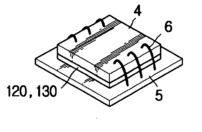
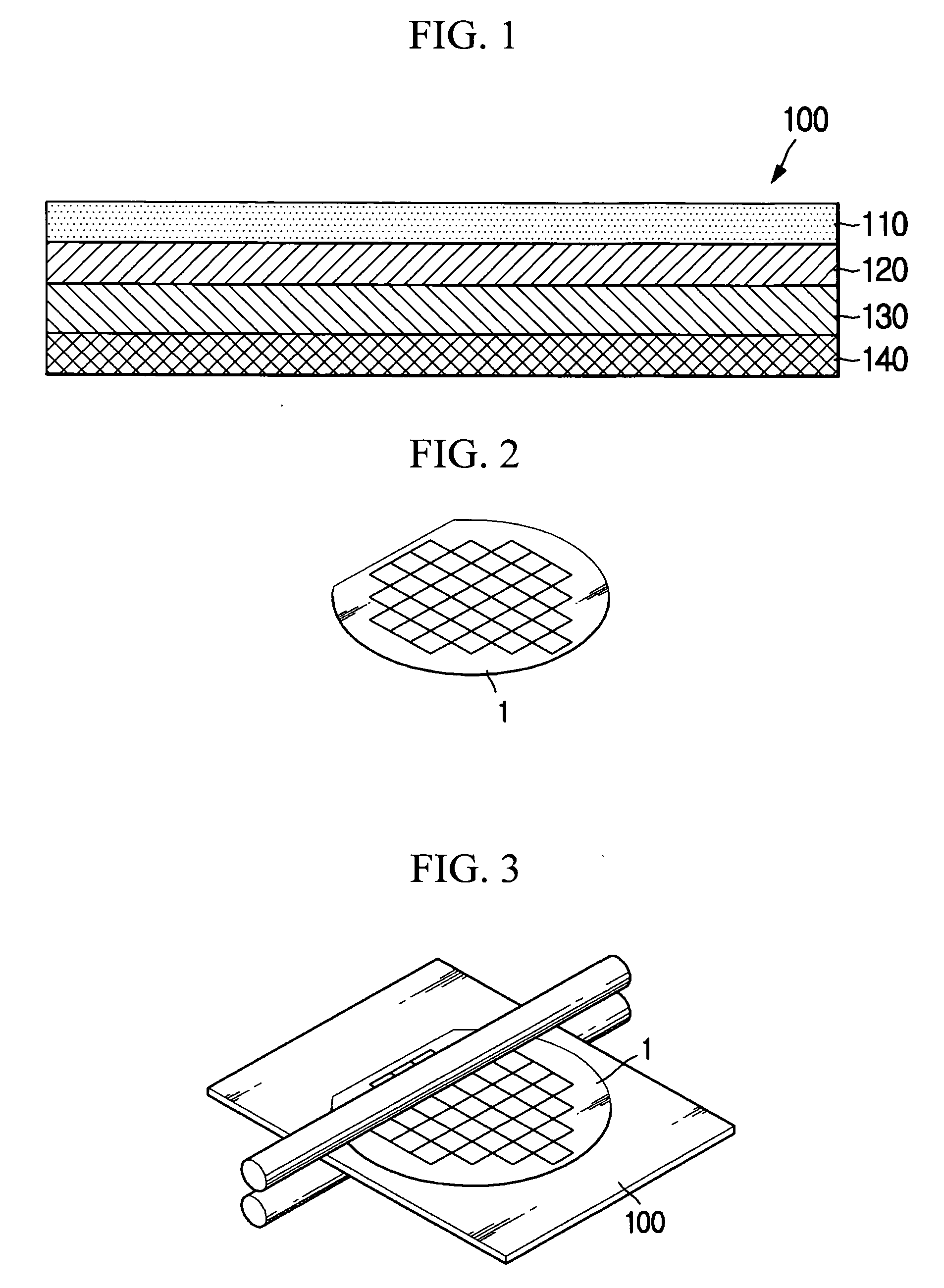
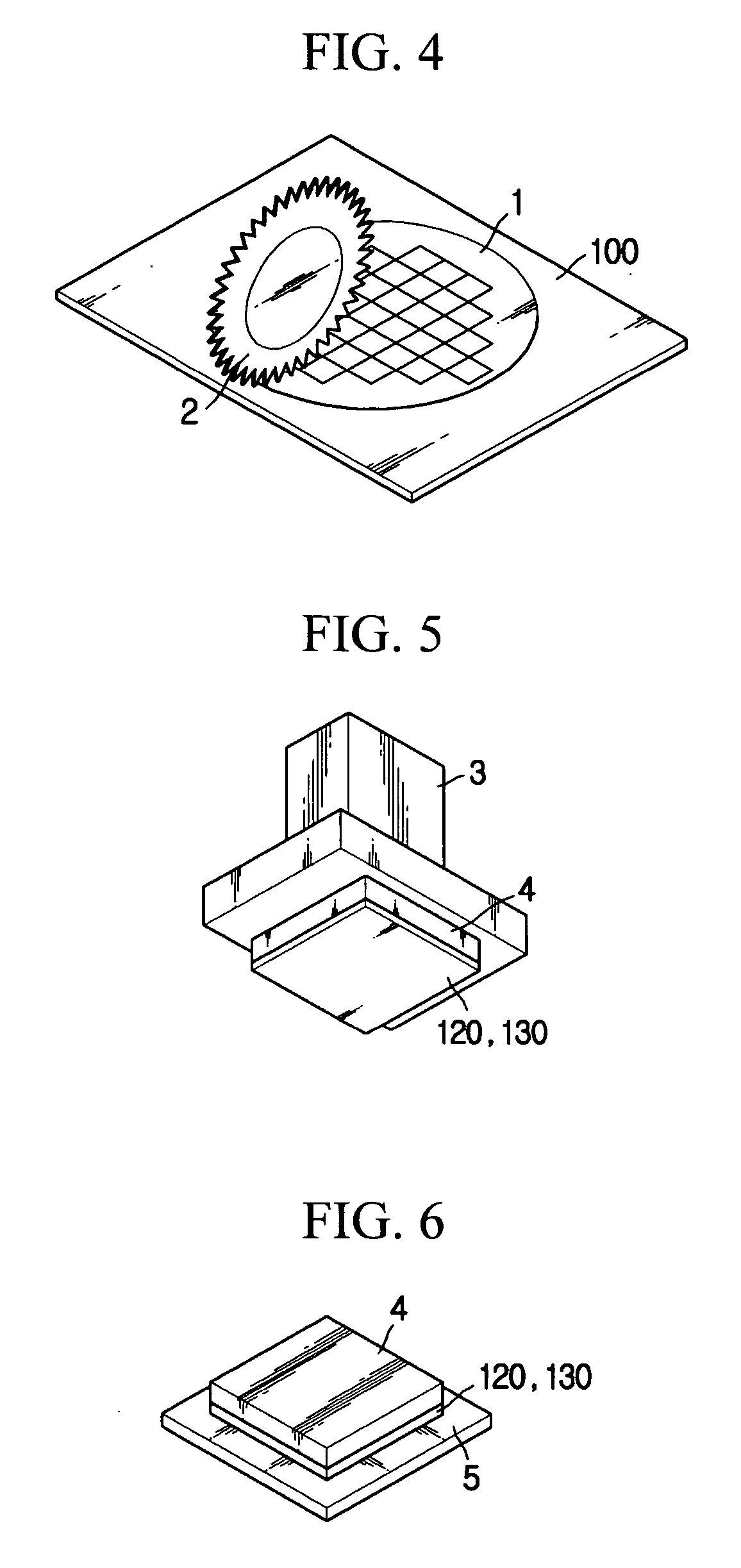
[0017]FIG. 1 is a cross-sectional view showing a dicing die adhesive film according to a preferred embodiment of the present invention.
[0018...
PUM
| Property | Measurement | Unit |
|---|---|---|
| storage modulus | aaaaa | aaaaa |
| storage modulus | aaaaa | aaaaa |
| temperature | aaaaa | aaaaa |
Abstract
Description
Claims
Application Information