Redundancy circuit in semiconductor memory device

Inactive Publication Date: 2006-11-02
SK HYNIX INC
View PDF4 Cites 9 Cited by
  • Summary
  • Abstract
  • Description
  • Claims
  • Application Information

AI Technical Summary

Benefits of technology

[0008] The present invention relates to a redundancy circuit in which a plurality of redundan

Problems solved by technology

However, since one redundant substitution unit is arranged in one fuse set according to the prior art redundancy circuit, there is a drawback that it is impossible to utilize the fuse set if there is any defect in the redundant substitution unit.
Meanwhile, although s

Method used


Image

  • Redundancy circuit in semiconductor memory device
  • Redundancy circuit in semiconductor memory device
  • Redundancy circuit in semiconductor memory device

Examples


first embodiment

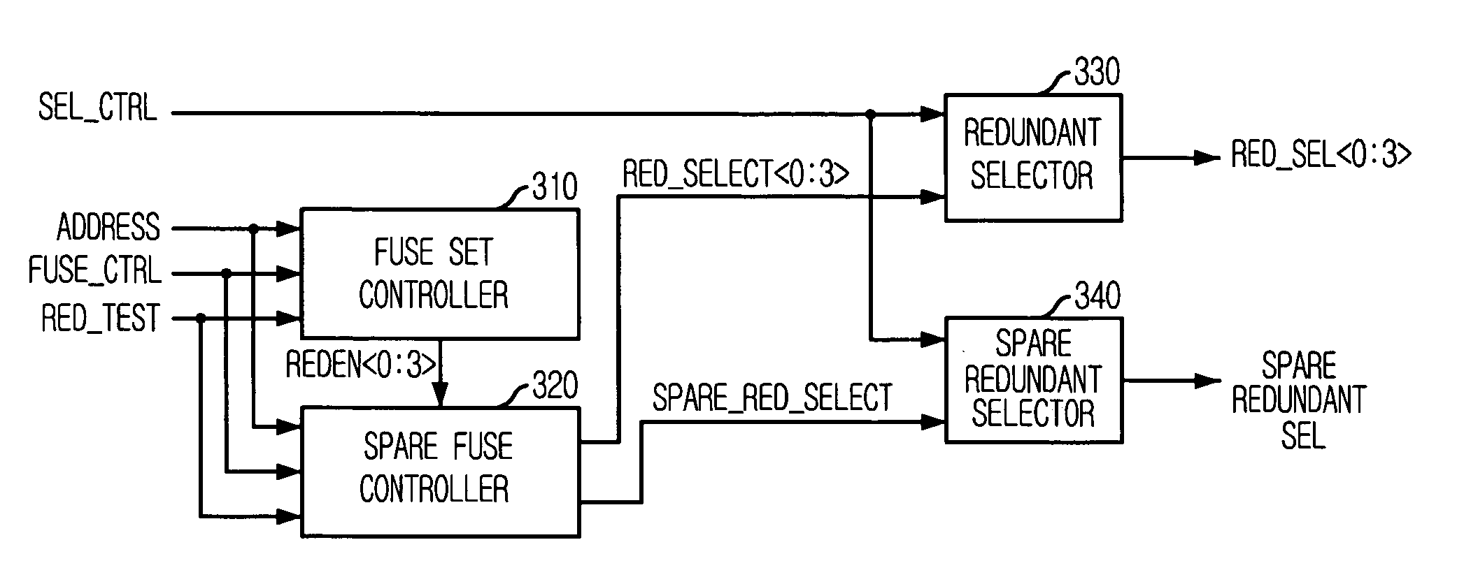
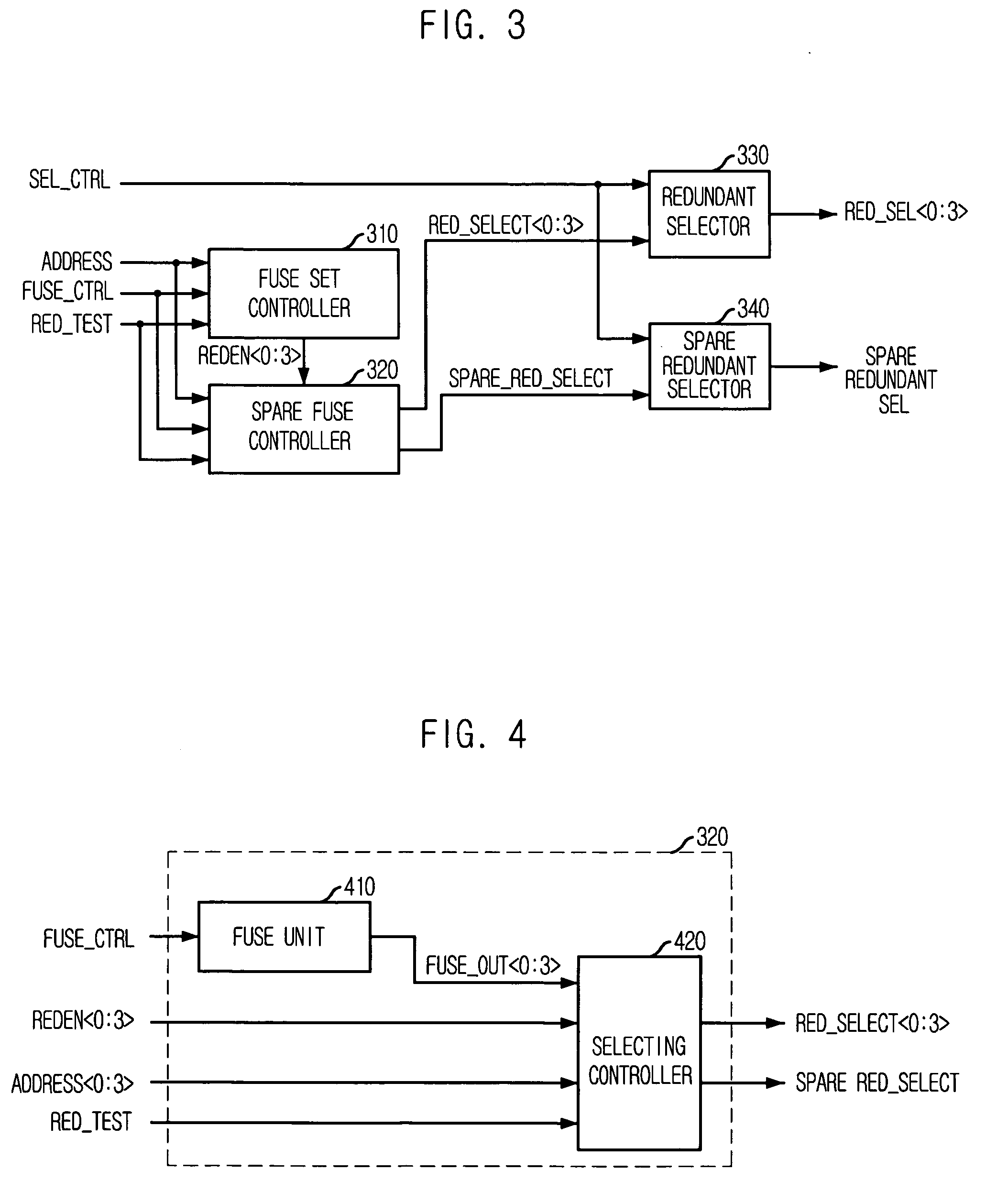
[0027]FIG. 3 is a block diagram setting forth a redundancy circuit in accordance with the present invention.

[0028] Referring to FIG. 3, the inventive redundancy circuit includes a fuse set controller 310, a spare fuse controller 320, a redundant selector 330, and a spare redundant selector 340.

[0029] In one embodiment of the present invention, the fuse set controller 310 of the present invention has the same constitution with that of the prior art redundancy circuit. The fuse set controller 310 outputs redundancy enable signals REDEN0:3> of logic high levels according to a predetermined combination of applied address signals ADDRESS.

[0030] The spare fuse controller 320 enables redundant selection control signals RED_SELECT0:3> or a spare redundant selection control signal SPARE RED_SELECT according to a fuse option in a normal mode. In addition, in a test mode, the spare fuse controller 320 may enable the redundant selection control signals RED_SELECT0:3> or the spare redundant se...

second embodiment

[0080]FIG. 12 is a block diagram setting forth a redundancy circuit in accordance with the present invention.

[0081] Referring to FIG. 12, the redundancy controller of the second embodiment comprises a fuse set controller 1210, a spare fuse unit 1220, a redundant selector 1230, and a multiplexer 1240.

[0082] In one embodiment of the present invention, the fuse set controller 1210 has the same constitution with that of the fuse set controller of FIG. 1, and outputs the redundancy enable signals REDEN0:3> which is enabled by a predetermined combination of applied address signals ADDRESS.

[0083] In one embodiment of the present invention, the spare fuse unit 1220 has the same configuration with that of the spare fuse unit of FIG. 5, and outputs the fuse-out signals FUSE_OUT0:3> of which logic levels are determined according to the connection state of the first and the second spare fuses FUSE1 and FUSE2.

[0084] The redundant selector 1230 which is controlled by the selection control sign...


PUM


Abstract

A redundancy circuit in a semiconductor memory device comprises a fuse set controller configured to output a redundancy enable signal enabled according to applied address signals; a redundant selector; a spare redundant selector; and a spare fuse controller configured to be controlled by the redundancy enable signal, and to output a selection control signal that selects at least one of the redundant selector and the spare redundant selector in accordance with an internal fuse option.

Description

CROSS REFERENCE TO RELATED APPLICATIONS [0001] The present application contains subject matter related to Korean patent application No. 2005-36227, filed in the Korean Patent Office on Apr. 29, 2005, the entire contents of which being incorporated herein by reference. BACKGROUND OF THE INVENTION [0002] The present invention relates to a semiconductor device; and, more particularly, to a redundancy circuit in a semiconductor memory device. [0003] In general, a semiconductor memory device undergoes a predetermined test in a wafer state so that undesired cells, word lines, bit lines or the like having errors or defects therein are sort out. Furthermore, the same test is also carried out for a redundancy circuit in order to find out defects. As is well known, the redundancy cell array is required in the semiconductor memory device in order for a cell in the redundancy cell array to perform a normal operation in place of an arbitrary cell in a normal cell array, if the arbitrary cell in ...

Claims


Application Information

Patent Timeline
IPC IPC(8): G11C29/00
CPCG11C29/838G11C29/787G11C29/00
Inventor KANG, SANG-HEE
Owner SK HYNIX INC
Why Eureka
Try Eureka