Multi-axis vacuum motor assembly

a vacuum motor and multi-axis technology, applied in the direction of motor/generator/converter stopper, dynamo-electric converter control, instruments, etc., can solve the problems of abrasion between, surface contamination of other wafers, and fragile silicon wafers by natur

Inactive Publication Date: 2006-11-02
APPLIED MATERIALS INC
View PDF31 Cites 36 Cited by
  • Summary
  • Abstract
  • Description
  • Claims
  • Application Information

AI Technical Summary

Problems solved by technology

Semiconductor wafers are by their nature fragile and easily chipped or scratched.
Vibration of the robot can cause abrasion between a robot blade holding a wafer and a surface of the wafer.
The “dust” or abraded particles of the wafer caused by such vibration can in turn cause surface contamination of other wafers.

Method used


Image

  • Multi-axis vacuum motor assembly
  • Multi-axis vacuum motor assembly
  • Multi-axis vacuum motor assembly

Examples


Embodiment Construction

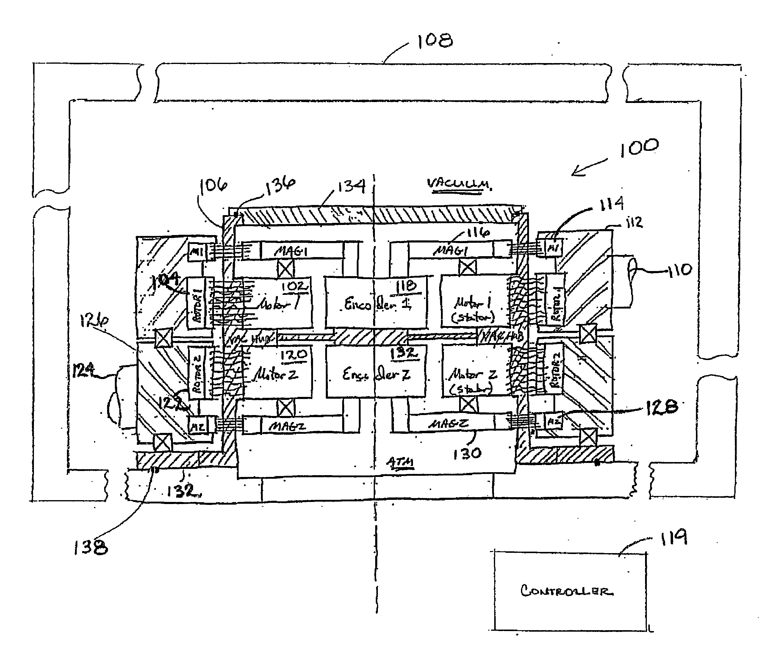
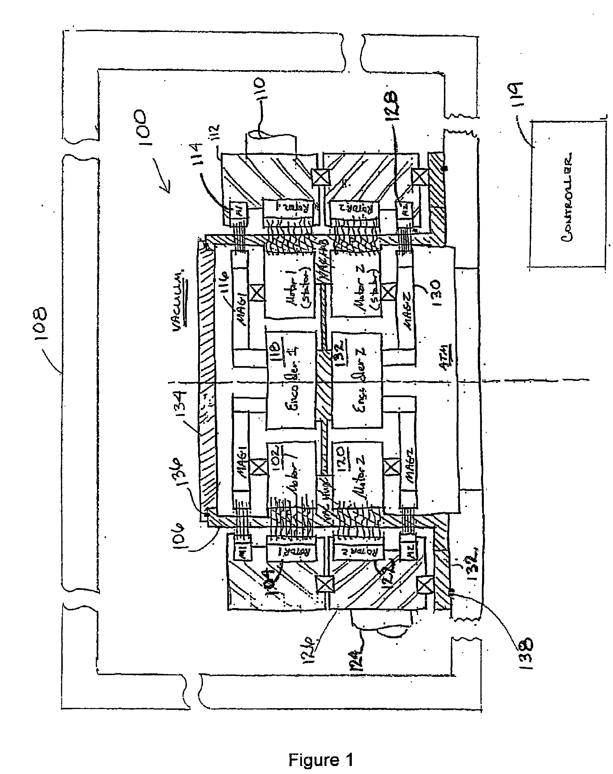
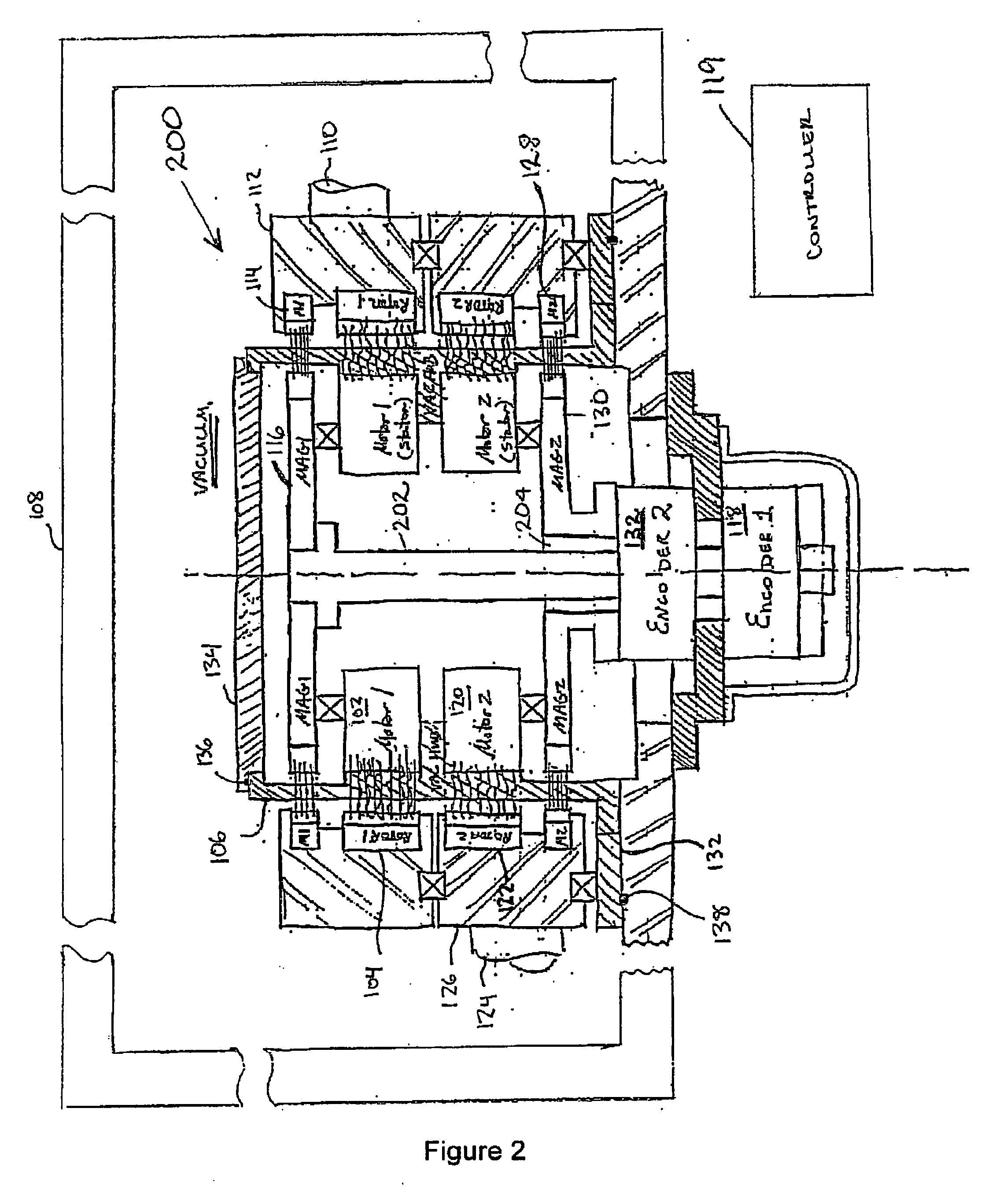
[0013] Disclosed is a multi-axis motor assembly for use in a transfer or other chamber. The improved design allows feedback devices and / or motor elements to be nested so as to reduce stack height below the transfer chamber. Additionally, sensing functions need not be transmitted across a vacuum barrier.

[0014]FIG. 1 is a cross-sectional view of a first exemplary multi-axis vacuum motor assembly 100 provided in accordance with the present invention. As will be described below, the first multi-axis motor assembly 100 utilizes magnetic coupling across a vacuum barrier to drive a robot in a vacuum chamber. Feedback devices and motor elements are nested for vertical compactness and reside outside of the vacuum chamber.

[0015] The first multi-axis vacuum motor assembly 100 of FIG. 1 includes a first stator 102 (Motor 1 (stator)) for driving a first rotor 104 (Rotor 1) across a vacuum barrier 106 of a vacuum chamber 108. The first stator 102 may act as an active magnetic coupling to drive ...


PUM


Abstract

In at least one aspect, a second multi-axis vacuum motor assembly is provided. The second multi-axis vacuum motor assembly includes (1) a first rotor; (2) a first stator adapted to commutate so as to rotate the first rotor across a vacuum barrier and control rotation of a first axis of a robot arm within a vacuum chamber; (3) a second rotor below the first rotor; (4) a second stator below the first stator and adapted to commutate so as to rotate the second rotor across the vacuum barrier and control rotation of a second axis of the robot arm within the vacuum chamber; (5) a first feedback device adapted to monitor rotation of the first axis of the robot arm; and (6) a second feedback device adapted to monitor rotation of the second axis of the robot arm. Numerous other aspects are provided.

Description

[0001] The present application claims priority from U.S. Provisional Patent Application Ser. No. 60 / 652,145, filed Feb. 12, 2005, which is hereby incorporated by reference herein in its entirety.FIELD OF THE INVENTION [0002] The present invention relates to semiconductor device manufacturing, and more particularly to a multi-axis motor assembly for use with a wafer handler. BACKGROUND OF THE INVENTION [0003] In the manufacture of semiconductor devices, such as integrated circuits (ICs), dynamic random access memories (DRAMs), etc., large thin wafers (typically of silicon) from which the semiconductor devices are fabricated must frequently be transferred from one processing chamber to another. This transfer of wafers must be carried out in a clean environment and often at sub-atmospheric pressures. To this end various mechanical arrangements have been devised for transferring wafers to and from processing chambers in a piece of equipment or from one piece of equipment to another. [00...

Claims


Application Information

Patent Timeline
Patent Type & Authority Applications(United States)
IPC IPC(8): B66C23/00
CPCB25J9/126B25J19/0079H01L21/68707H02K16/00H02K7/09H02K7/14H02K5/128
Inventor HUDGENS, JEFFREY C.
Owner APPLIED MATERIALS INC
Why Eureka
Try Eureka