Method for making integrated circuits

a technology of integrated circuits and manufacturing methods, applied in the direction of semiconductor/solid-state device manufacturing, basic electric elements, electric devices, etc., can solve the problems of reducing the performance of integrated circuits, requiring several interconnected levels of wiring, and negating some performance advantages

Inactive Publication Date: 2006-11-02
MICRON TECH INC
View PDF99 Cites 18 Cited by
  • Summary
  • Abstract
  • Description
  • Claims
  • Application Information

AI Technical Summary

Problems solved by technology

The complexity of some integrated circuits demand several interconnected levels of wiring.
(The diffusion barrier is generally necessary because copper atoms readily diffuse through common insulators, such as silicon dioxide, resulting in unreliable or inoperative integrated circuits.)
The first is that typical copper-diffusion barriers add appreciable resistance to the copper wiring, and thus negate some promised performance advantages.
And, the second is that the number of separate procedures or steps necessary to make the copper wiring using the extended technique makes fabrication both costly and time consuming.

Method used


Image

  • Method for making integrated circuits
  • Method for making integrated circuits
  • Method for making integrated circuits

Examples


Embodiment Construction

[0018] The following detailed description, which references and incorporates FIGS. 1-8, describes and illustrates specific embodiments of the invention. These embodiments, offered not to limit but only to exemplify and teach the concepts of the invention, are shown and described in sufficient detail to enable those skilled in the art to implement or practice the invention. Thus, where appropriate to avoid obscuring the invention, the description may omit certain information known to those of skill in the art.

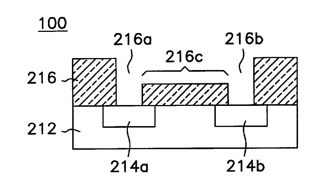
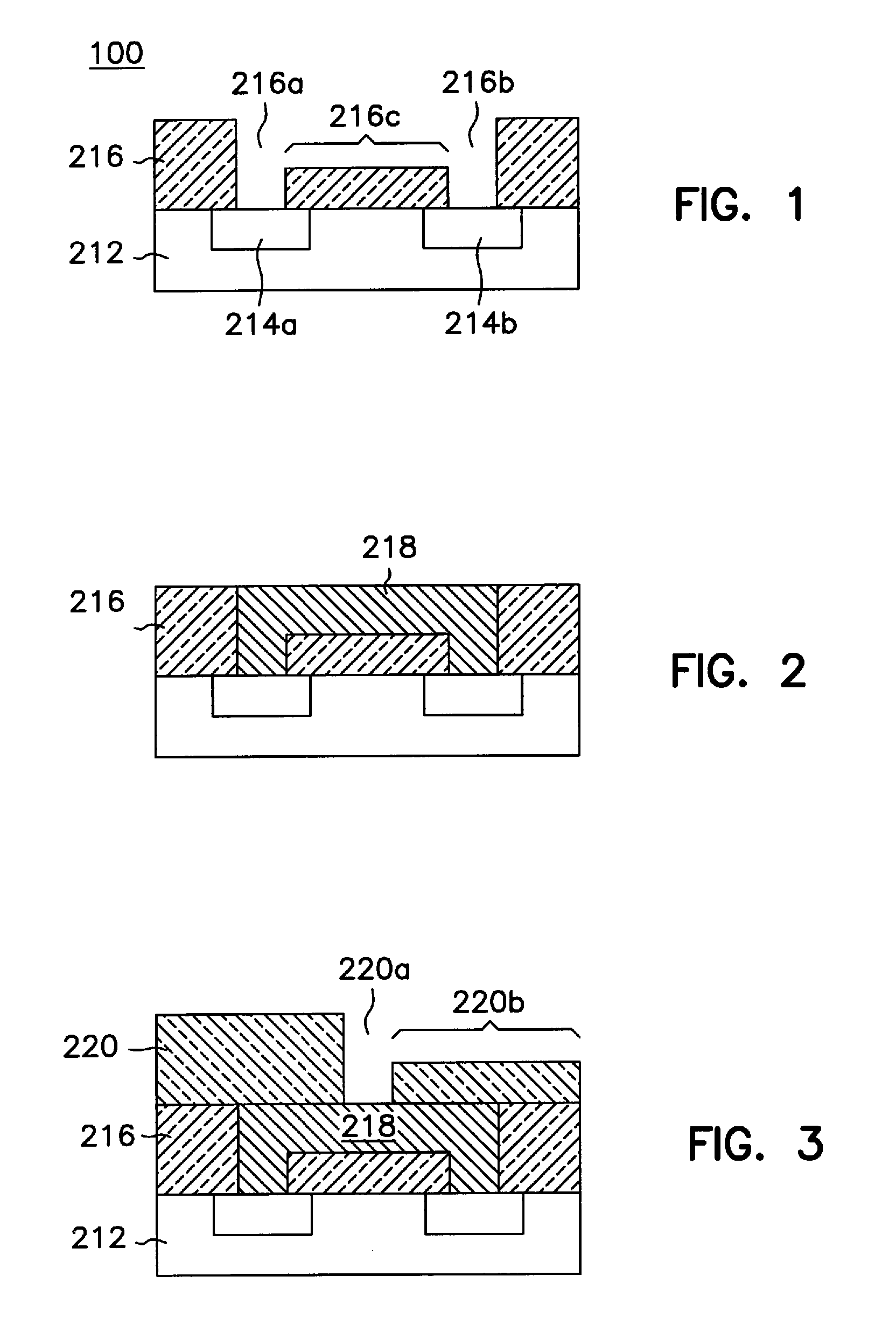
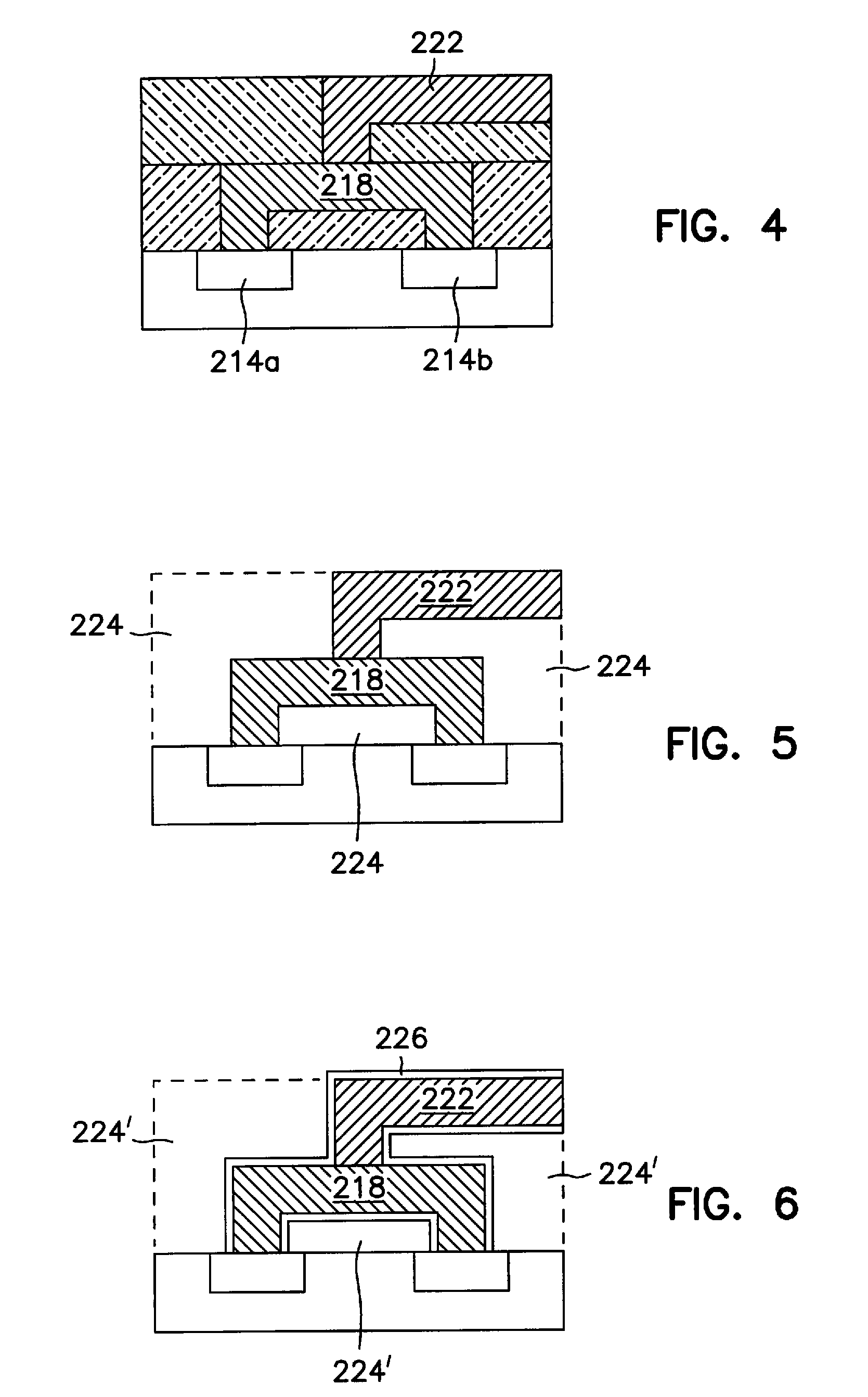
[0019]FIGS. 1-7 show a number of cross-sectional views of a partial integrated-circuits assembly 100, which taken collectively and sequentially, illustrate a unique exemplary method of making integrated circuits, and more particularly making integrated-circuit wiring in accord with teachings of the present invention. The method, as shown in FIG. 1, begins with a known integrated-circuit assembly or structure 100, which can exist within any integrated circuit, a dynamic-random-a...


PUM

PropertyMeasurementUnit
thicknessaaaaaaaaaa
thicknessaaaaaaaaaa
thickaaaaaaaaaa

Abstract

Integrated circuits, the key components in thousands of electronic and computer products, include interconnected networks of electrical components. The components are typically wired, or interconnected, together with aluminum wires. In recent years, researchers have begun using copper instead of aluminum to form integrated-circuit wiring, because copper offers lower electrical resistance and better reliability at smaller dimensions. However, copper typically requires use of a diffusion barrier to prevent it from contaminating other parts of an integrated circuit. Unfortunately, typical diffusion barrier materials add appreciable resistance to the copper wiring, and thus negate some advantages of using copper. Moreover, conventional methods of forming the copper wiring are costly and time consuming. Accordingly, the inventors devised one or more exemplary methods for making integrated-circuit wiring from materials, such as copper-, silver-, and gold-based metals. One exemplary method removes two or more masks in a single removal procedure, forms a low-resistance diffusion barrier on two or more wiring levels in a single formation procedure, and fills insulative material around and between two or more wiring levels in a single fill procedure. This and other embodiments hold the promise of simplifying fabrication of integrated-circuit wiring dramatically.

Description

RELATED APPLICATIONS [0001] This application is a Continuation of U.S. application Ser. No. 09 / 484,303, filed Jan. 18, 2000, which is incorporated herein be reference.TECHNICAL FIELD [0002] The present invention concerns methods of semiconductor device or integrated circuit manufacturing, particularly methods of forming interconnects from copper and other metals. BACKGROUND OF THE INVENTION [0003] Integrated circuits, the key components in thousands of electronic and computer products, are interconnected networks of electrical components fabricated on a common foundation, or substrate. Fabricators typically use various techniques, such as layering, doping, masking, and etching, to build thousands and even millions of microscopic resistors, transistors, and other electrical components on a silicon substrate, known as a wafer. The components are then wired, or interconnected, together with aluminum wires to define a specific electric circuit, such as a computer memory. The aluminum wi...

Claims


Application Information

Patent Timeline
Patent Type & Authority Applications(United States)
IPC IPC(8): H01L21/302H01L21/461H01L21/285H01L21/768
CPCH01L21/28512H01L21/76885H01L21/76856H01L21/76852
Inventor AHN, KIE Y.FORBES, LEONARD
Owner MICRON TECH INC
Why Eureka
Try Eureka