

High-density nonvolatile memory array fabricated at low temperature comprising semiconductor diodes
a memory array and low temperature technology, applied in the direction of diodes, semiconductor devices, semiconductor/solid-state device details, etc., can solve the problems of copper having even lower thermal tolerance and wires tend to soften
- Summary
- Abstract
- Description
- Claims
- Application Information
AI Technical Summary
Benefits of technology
Problems solved by technology
Method used
Image

Examples
example
Copper Conductors
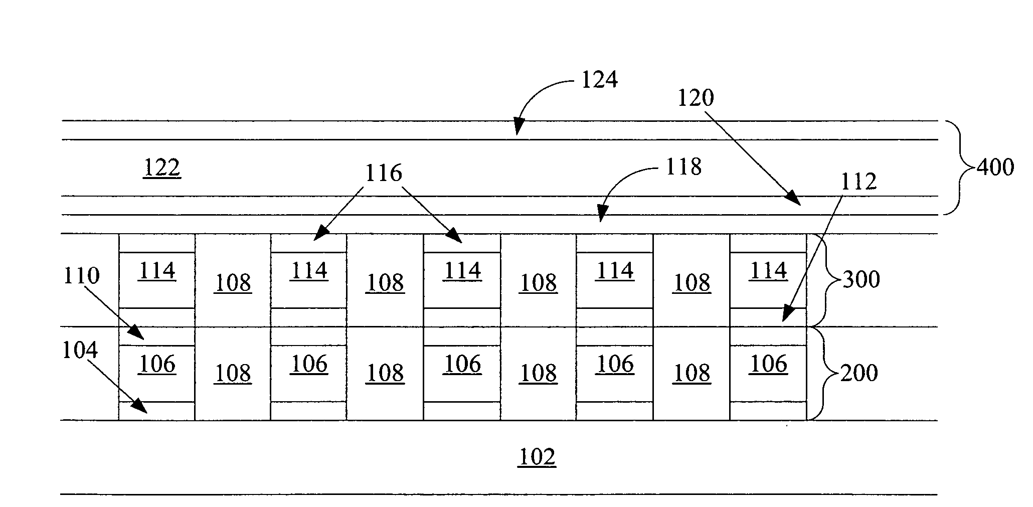
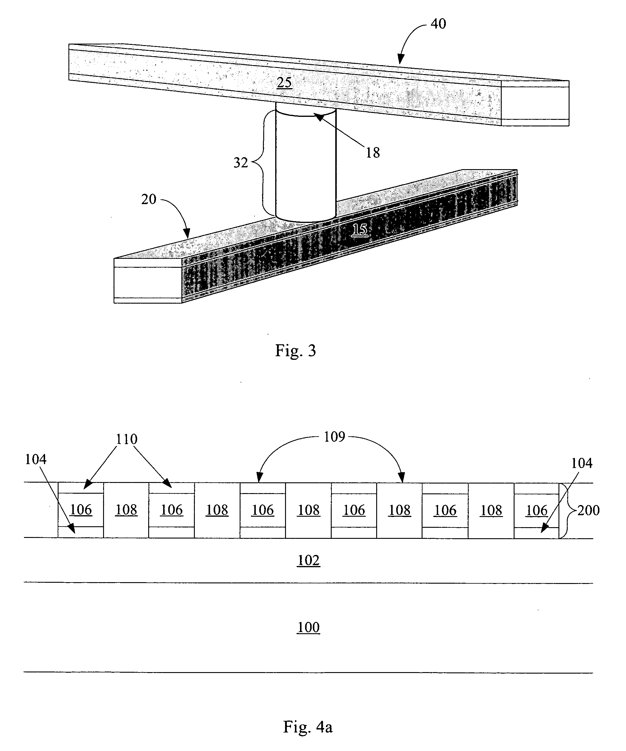
[0067] Turning to FIG. 5a, in this embodiment, fabrication begins as before over substrate 100 and insulating layer 102, which may be as described in the previous embodiment.
[0068] In preferred embodiments a think layer 201 of, for example, silicon nitride is deposited on insulating layer 102. This layer will serve as an etch stop during the damascene etch to come.
[0069] Next a thick layer 202 of a dielectric, for example TEOS, is deposited. Its thickness may be between about 1000 and about 6000 angstroms, preferably about 4000 angstroms. A conventional damascene etch is performed to etch substantially parallel trenches 204. The etch stops on silicon nitride layer 201. A barrier layer 206 of, for example, tantalum nitride, tantalum, tungsten, tungsten nitride, titanium nitride, or any other appropriate material is conformally deposited covering dielectric layer 202 and lining trenches 204.
[0070] As shown in FIG. 5b, next copper layer 208 is deposited on barrier ...
PUM
 Abstract
Description
Claims
Application Information