Surface passivated photovoltaic devices

a photovoltaic device and surface technology, applied in the field of photovoltaic devices, can solve the problems of significant energy loss, production of such devices may not always provide a viable option to meet all customer demands, etc., and achieve the effect of reducing potential barriers

Inactive Publication Date: 2006-11-16
GENERAL ELECTRIC CO
View PDF7 Cites 245 Cited by
  • Summary
  • Abstract
  • Description
  • Claims
  • Application Information

AI Technical Summary

Benefits of technology

[0006] In accordance with one aspect of the present technique, a photovoltaic device comprising a photovoltaic cell and a back surface passivated structure is provided. The photovoltaic cell includes an emitter layer comprising a crystalline semiconductor material. Further, the photovoltaic cell includes a lightly doped crystalline substrate disposed adjacent the emitter layer, where the lightly doped crystalline substrate comprises a single crystal or a poly crystal semiconductor material and where the lightly doped crystalline substrate and the emitter layer are oppositely doped. The photovoltaic device also includes a back surface passivated structure comprising a highly doped back surface field layer disposed adjacent the lightly doped crystalline substrate, where the highly doped back surface field layer includes a doped amorphous or a doped microcrystalline semiconductor material, wherein the highly dop

Problems solved by technology

However, due to the high cost that is often involved in making solar cells, production of such devices may not always provide a viable option to meet all customer demands.
However, vari

Method used


Image

  • Surface passivated photovoltaic devices
  • Surface passivated photovoltaic devices
  • Surface passivated photovoltaic devices

Examples


Embodiment Construction

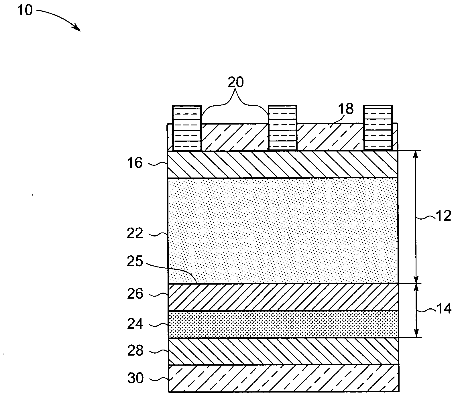
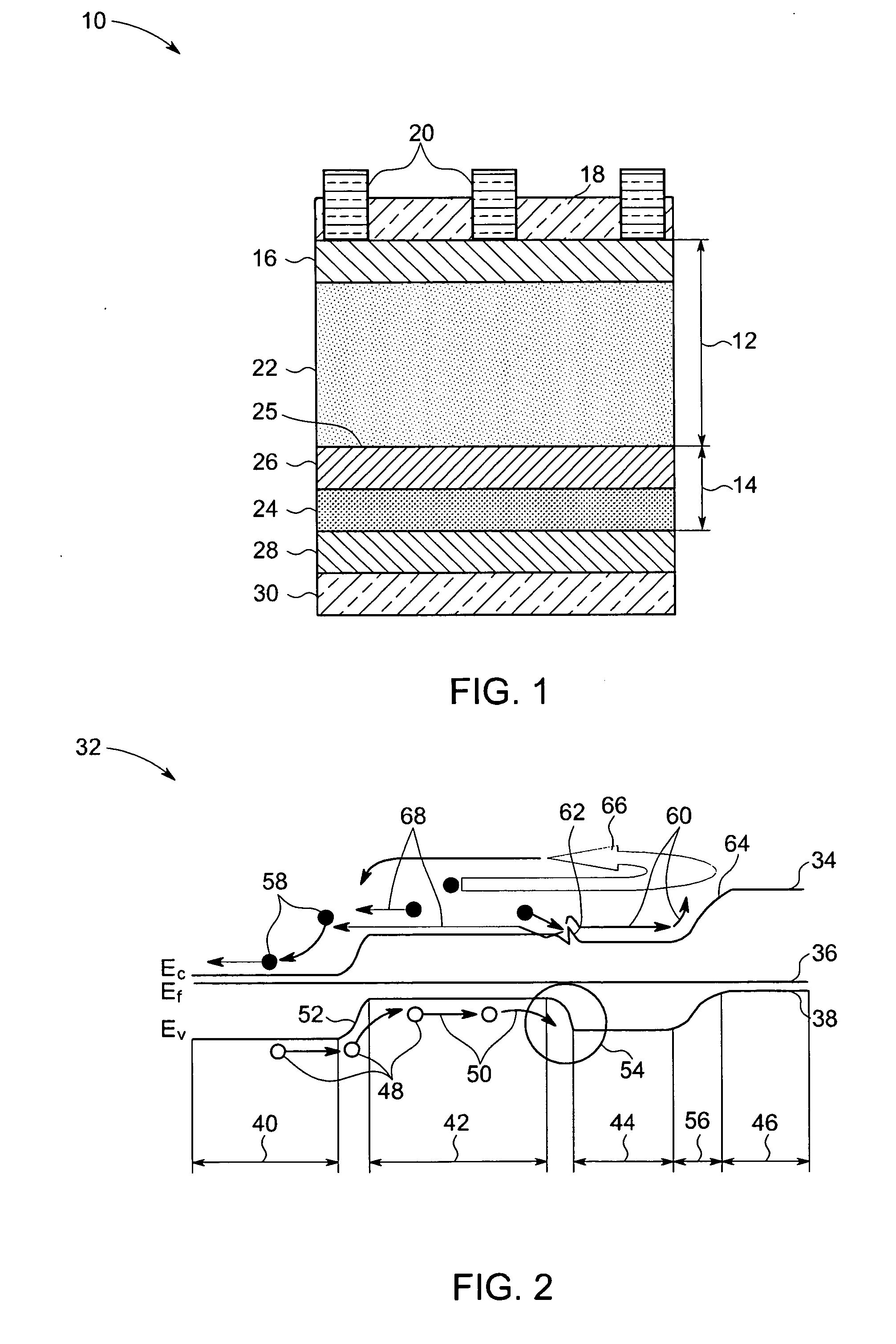
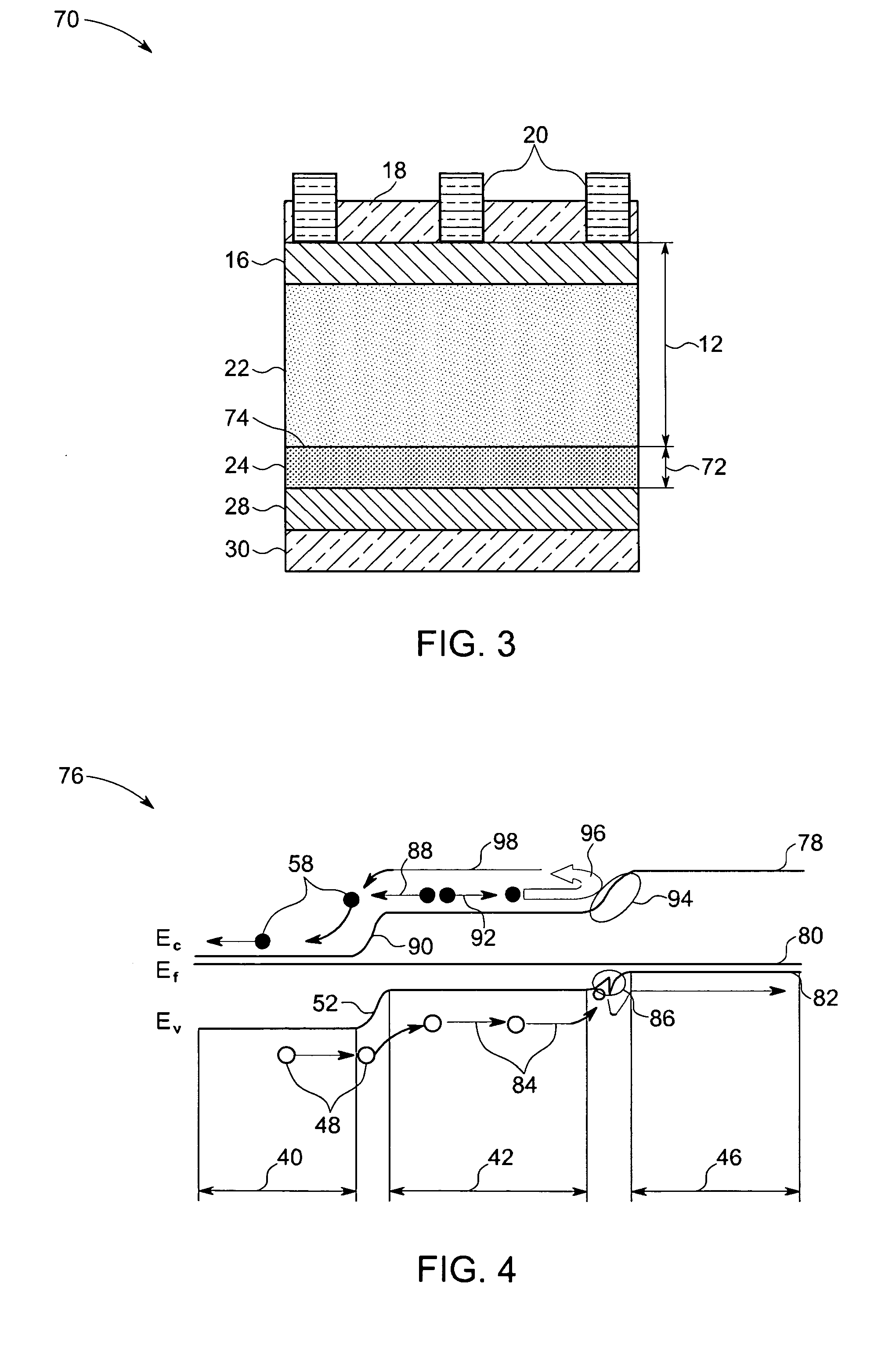
[0019] Typically, the structure of a photovoltaic device includes a first layer of one doped type and a second layer of the other doped type or a base layer and an emitter layer disposed between two current collection electrodes. As will be appreciated by those skilled in the art, when light is incident on the photovoltaic device, electron-hole pairs are generated which are then pulled across the junction of the layers of two doped types towards respective electrodes and contribute to the electric current produced by the device. In order to increase the efficiency of the device, it is usually desirable to prevent recombination of charge carriers, such as electrons and holes, generated within the device from the photovoltaic reaction, and to enable collection of the charge carriers at respective electrodes. In accordance with certain aspects of the present technique, the carrier generation / transport layer may include a lightly doped crystalline substrate. In certain embodiments, the ...


PUM


Abstract

A photovoltaic device comprising a photovoltaic cell is provided. The photovoltaic cell includes an emitter layer comprising a crystalline semiconductor material and a lightly doped crystalline substrate disposed adjacent the emitter layer. The lightly doped crystalline substrate and the emitter layer are oppositely doped. Further, the photovoltaic device includes a back surface passivated structure coupled to the photovoltaic cell. The structure includes a highly doped back surface field layer disposed adjacent the lightly doped crystalline substrate. The highly doped back surface field layer includes an amorphous or a microcrystalline semiconductor material, wherein the highly doped back surface field layer and the lightly doped crystalline substrate are similarly doped, and wherein a doping level of the highly doped back surface field layer is higher than a doping level of the lightly doped crystalline substrate. Additionally, the structure may also include an intrinsic back surface passivated layer disposed adjacent the lightly doped crystalline substrate, where the intrinsic back surface passivated layer includes an amorphous or a microcrystalline semiconductor material.

Description

BACKGROUND [0001] The invention relates generally to photovoltaic devices. More particularly, the invention relates to surface passivated photovoltaic devices having improved conversion efficiency and light confining properties. [0002] Photovoltaic devices, such as solar cells, convert incident electromagnetic radiations into electrical energy. The performance of these devices is measured in terms of their efficiency to convert these incident radiations into electrical energy. [0003] Photovoltaic devices are an environmentally friendly way of producing energy. As such, these devices may provide an increasingly useful option for supplying energy in the future. However, due to the high cost that is often involved in making solar cells, production of such devices may not always provide a viable option to meet all customer demands. [0004] High efficiency solar cells offer an alternative method of cost reduction. In other words, the more power a solar cell can generate, the fewer number ...

Claims


Application Information

Patent Timeline
IPC IPC(8): H01L33/00H01L31/068H01L31/078
CPCH01L31/02168H01L31/068H01L31/0745H01L31/056Y02E10/52Y02E10/547H01L31/078H01L31/0747
Inventor MANIVANNAN, VENKATESANEBONG, ABASIFREKE UDOJEFFREY HUANG, JIUNN-RUFEIST, THOMAS PAULJOHNSON, JAMES NEIL
Owner GENERAL ELECTRIC CO
Why Eureka
Try Eureka