Light emitting element mounting frame and light emitting device
- Summary
- Abstract
- Description
- Claims
- Application Information
AI Technical Summary
Benefits of technology
Problems solved by technology
Method used
Image

Examples
embodiment 1
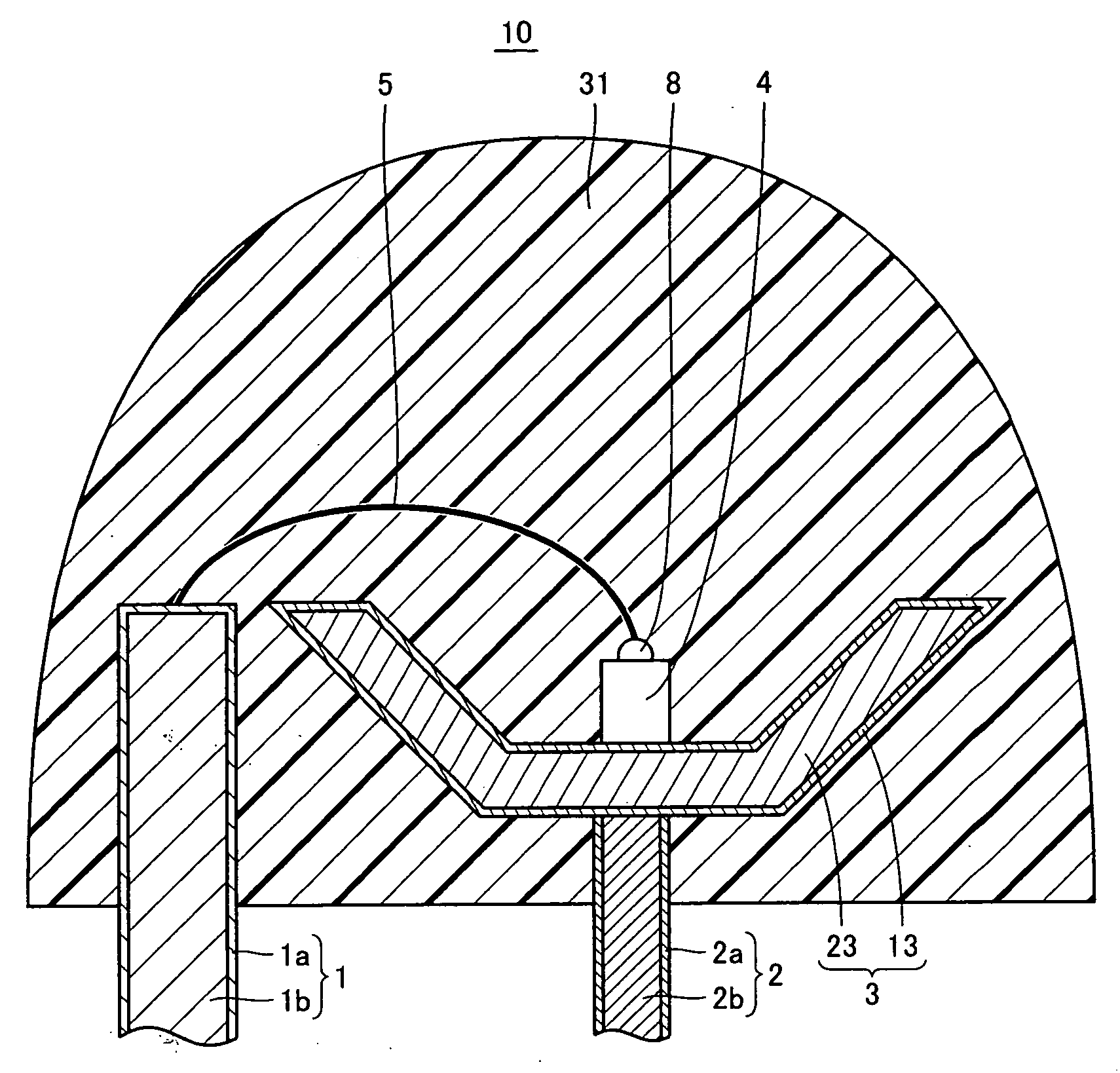
[0042]FIG. 1 is a schematic cross-sectional view of a light emitting device including copper lead frames 1, 2 and 3 having an Ag—Nd (0.7 at %) layer formed thereon, in accordance with Embodiment 1 of the present invention. Light emitting device 10 in accordance with the present embodiment includes a light emitting element 4, an inner lead 1 having a silver alloy layer 1a formed on an inner lead body 1b, a mount lead 2 having a silver alloy layer 2a formed on a mount lead body 2b, and a cup portion 3 surrounding light emitting element 4, having a silver alloy layer 13 formed on a cup portion body 23. At a bottom of cup portion 3, light emitting element 4 is mounted using Ag paste (not shown). Here, the silver alloy formed on the surface of these portions is Ag—Nd (0.7 at %), and its thickness is 100 nm. The Ag—Nd (0.7 at %) layer is formed by plating.
[0043] On light emitting element 4, n-type and p-type pad electrodes 7, 8 are formed, which are bonded with gold bonding wires 5 and 6...
embodiment 2
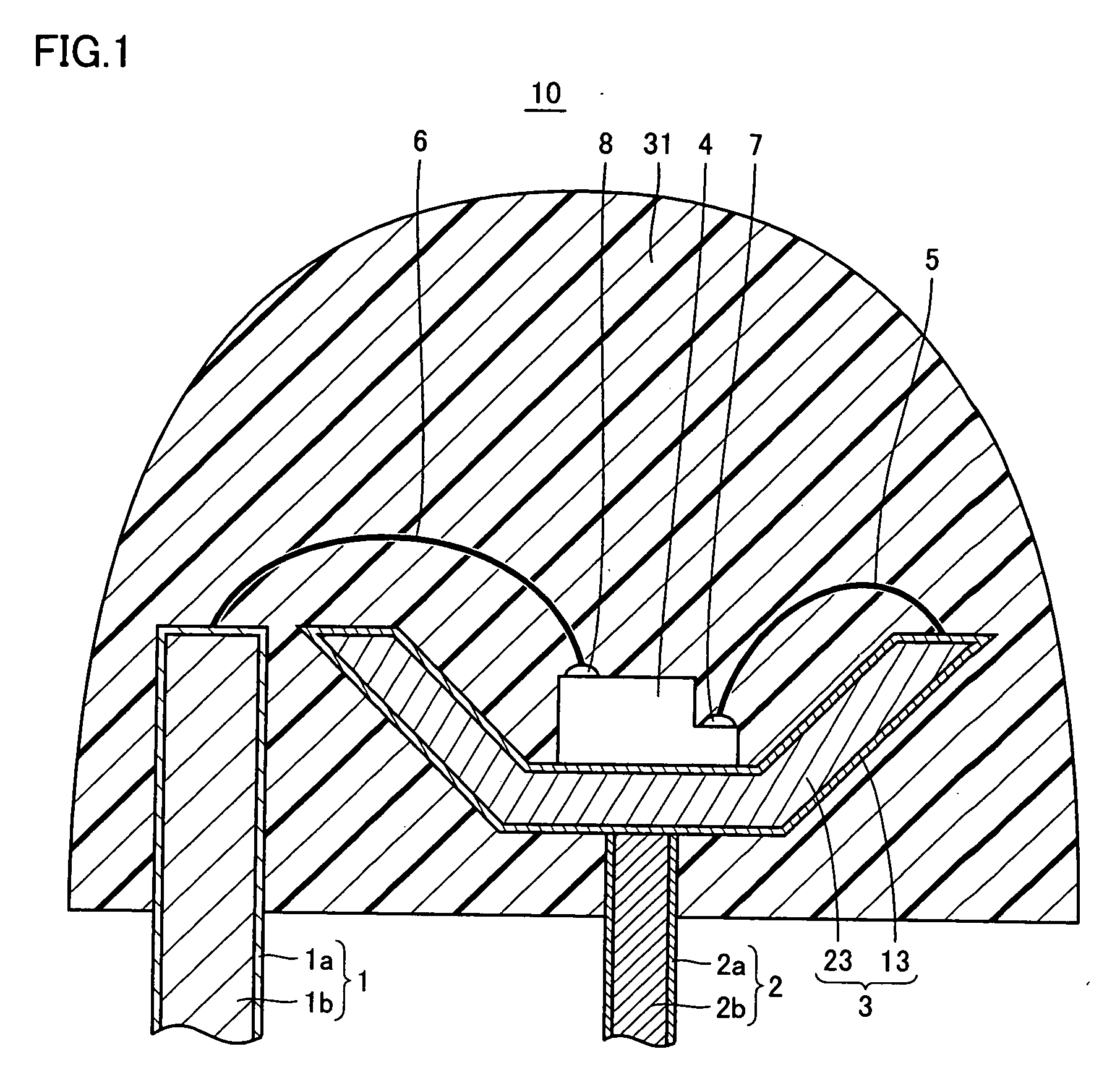
[0045]FIG. 2 is a schematic cross-sectional view of a light emitting device including silver-plated copper lead frames in accordance with Embodiment 2 of the present invention. Light emitting device 10 in accordance with the present embodiment includes light emitting element 4, inner lead 1, mount lead 2, and cup portion 3 for mounting light emitting element 4. At a bottom of mounting cup portion 3, light emitting element 4 is mounted using Ag paste (not shown). Here, on a side surface of cup portion 3, a silver alloy layer 13a is formed. Silver alloy layer 13a is of Ag—Nd (0.25 at %), and the thickness is 150 nm. The Ag—Nd (0.25 at %) is formed by plating.
[0046] On light emitting element 4, n-type and p-type pad electrodes 7, 8 are formed, which are bonded with gold bonding wires 5 and 6, to attain electrical conduction to the outside. Then, a mold member 31 is formed in the shape of a convex lens, to cover cup portion 3 for mounting light emitting element 4, light emitting elemen...
embodiment 3
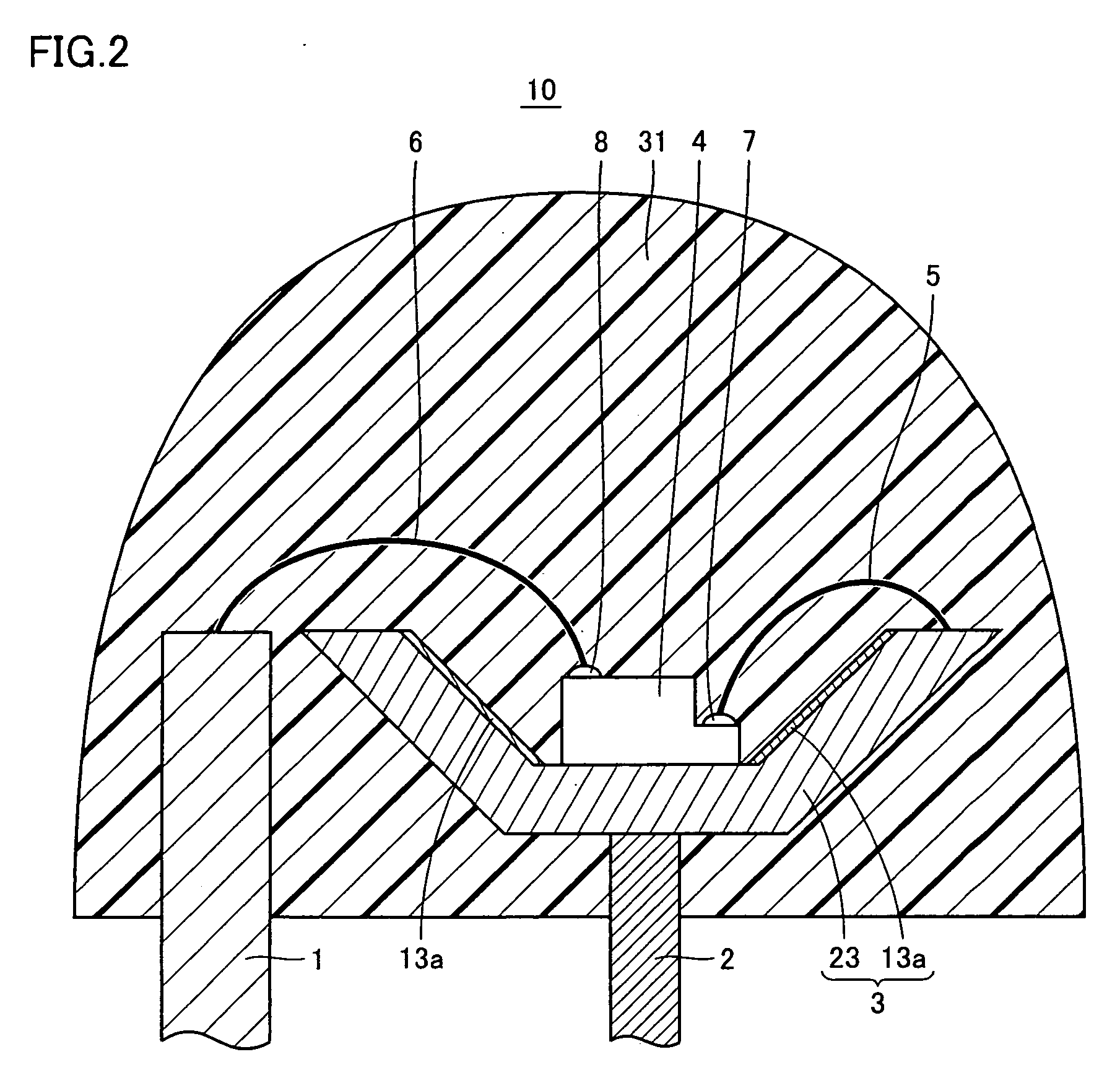
[0048]FIG. 3 is a schematic cross-sectional view of a light emitting device including silver-plated copper lead frames in accordance with Embodiment 3 of the present invention. Light emitting device 10 in accordance with the present embodiment includes light emitting element 4, inner lead 1, mount lead 2, and cup portion 3 for mounting light emitting element 4. Here, a silver alloy layer 13a is formed on a side surface of cup portion 3, and a silver alloy layer 13b is formed at the bottom of cup portion 3. As silver alloy layers 13a and 13b, Ag—Nd (1.0 at %) is used, and the thickness is 200 nm. At a bottom 32 of cup portion 3 for mounting, light emitting element 4 is mounted, using Ag paste. The Ag—Nd (1.0 at %) layer is formed by plating.
[0049] On the light emitting element, n-type and p-type pad electrodes 7, 8 are formed, which are bonded with gold bonding wires 5 and 6, to attain electrical conduction to the outside. Then, a mold member 31 is formed in the shape of a convex le...
PUM
 Abstract
Description
Claims
Application Information
 - Generate Ideas
- Intellectual Property
- Life Sciences
- Materials
- Tech Scout
- Unparalleled Data Quality
- Higher Quality Content
- 60% Fewer Hallucinations
Browse by: Latest US Patents, China's latest patents, Technical Efficacy Thesaurus, Application Domain, Technology Topic, Popular Technical Reports.
© 2025 PatSnap. All rights reserved.Legal|Privacy policy|Modern Slavery Act Transparency Statement|Sitemap|About US| Contact US: help@patsnap.com