Methods for processing, optimization, calibration and display of measured dielectrometry signals using property estimation grids

Inactive Publication Date: 2006-11-23
GOLDFINE NEIL J +4
View PDF44 Cites 13 Cited by
  • Summary
  • Abstract
  • Description
  • Claims
  • Application Information

AI Technical Summary

Benefits of technology

[0013] A preferred embodiment of the method according to the invention includes the incorporation of geometric properties into the grid databases for the representation of multi-layered media and the use of analytic properties of the measurement grid to map from measurement space to property space, such as singular value decomposition, condition numbers (and visualizations of these), to improve selection amongst alternative sensor designs and operating conditions. In addition, the preferred embodiment uses methods for measuring with and calibrating dielectrometers, using single and multiple grids for multiple wavenumber dielectrometry Exploiting the characterization and understanding of other properties of such mappings to aid in choosing and selecting among measurement grid alternatives is also feasible.
[0015] The need is also recognized for a sensor device configuration that reduce the sensor sensitivity to undesired inhomogenities across the face of the sensor. In a preferred embodiment, a sensor has multiple electric field penetration depths but each with the same air-gap, fluid gap, or shim lift-off height, thereby greatly reducing the number of unknowns in parameter estimation algorithms.

Problems solved by technology

These defects can be created during the manufacturing process, such as improper curing or incorrect layer thickness for stratified media, or when the material is placed into service by use- and / or age-related degradation processes, such as fatigue.
In many applications both sides of the MUT are not easily accessible and single-sided sensor configurations are required.
However, the determination of solid dielectric properties is more complicated due to the presence of microcavities or unintentional air gaps between the solid dielectric and the sensor.
Therefore, effective compensation may be difficult to achieve even with multiple sensors placed onto a single substrate.
One of the difficulties is due to the fact that a sensor having a number of sensor elements, each with different electrode spacings, those sensor elements are not co-located and therefore are not located at exactly the same places relative to the MUT.
Such inverse parameter estimation problems generally require numerical iterations of the forward problem, which can be very time consuming often preventing material identification in real-time.
In some cases, simple calibration procedures can be applied, but these suffer from requiring and assuming independent knowledge about the properties.
More advanced model-based techniques utilize multivariable parameter estimation algorithms to estimate the properties of interest, but these are generally slow, precluding real-time measurement capabilities, and may not converge on the desired solution.

Method used


Image

  • Methods for processing, optimization, calibration and display of measured dielectrometry signals using property estimation grids
  • Methods for processing, optimization, calibration and display of measured dielectrometry signals using property estimation grids
  • Methods for processing, optimization, calibration and display of measured dielectrometry signals using property estimation grids

Examples


Embodiment Construction

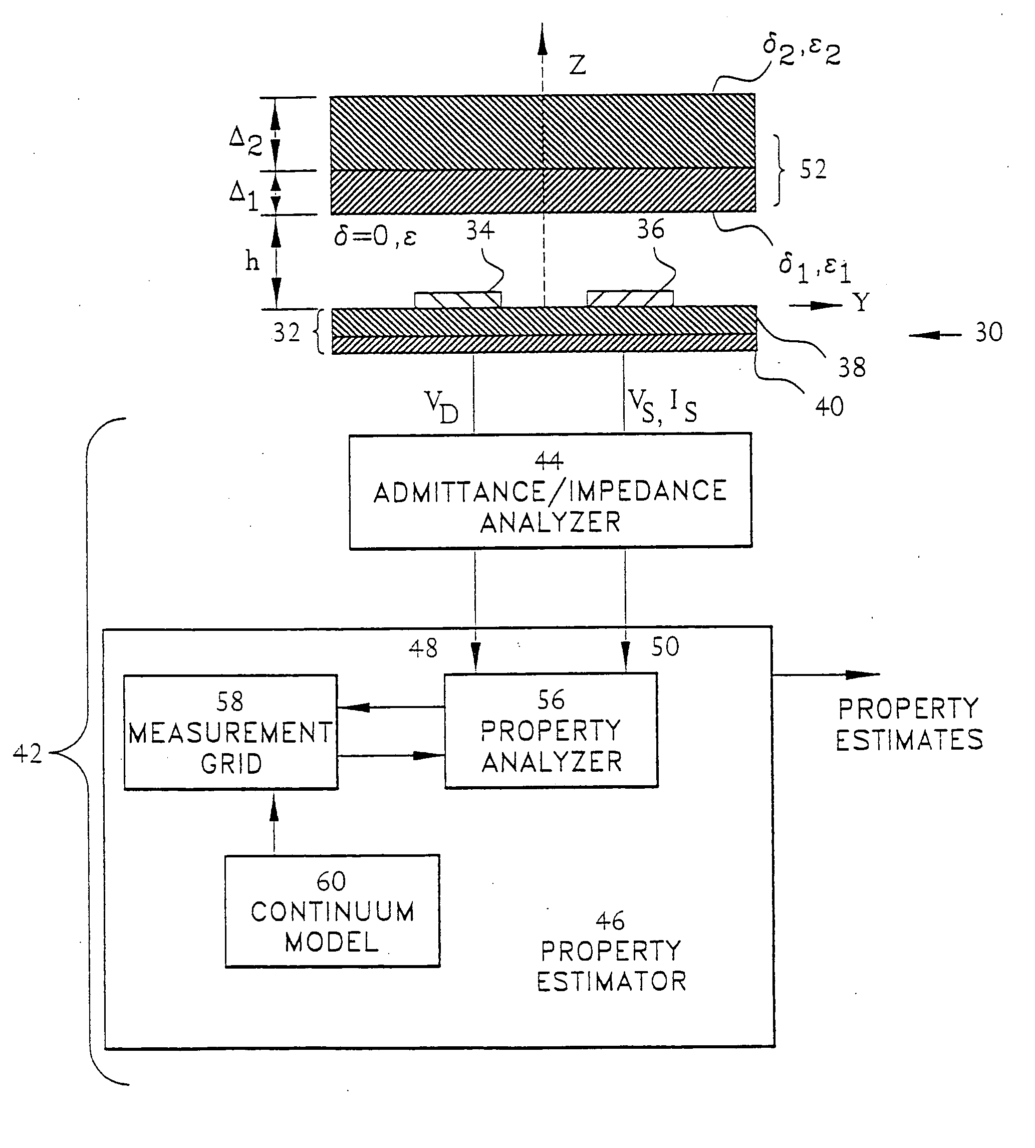
[0040] Methods, techniques, and devices are disclosed for measurements of electrical, physical, and dimensional properties of a material under test as well as geometric and kinematic properties of the measurement arrangement. These measurements are made with both contact and non-contact of the material under test by a sensor. For contact measurements, the sensor may be embedded in material under test (MUT).

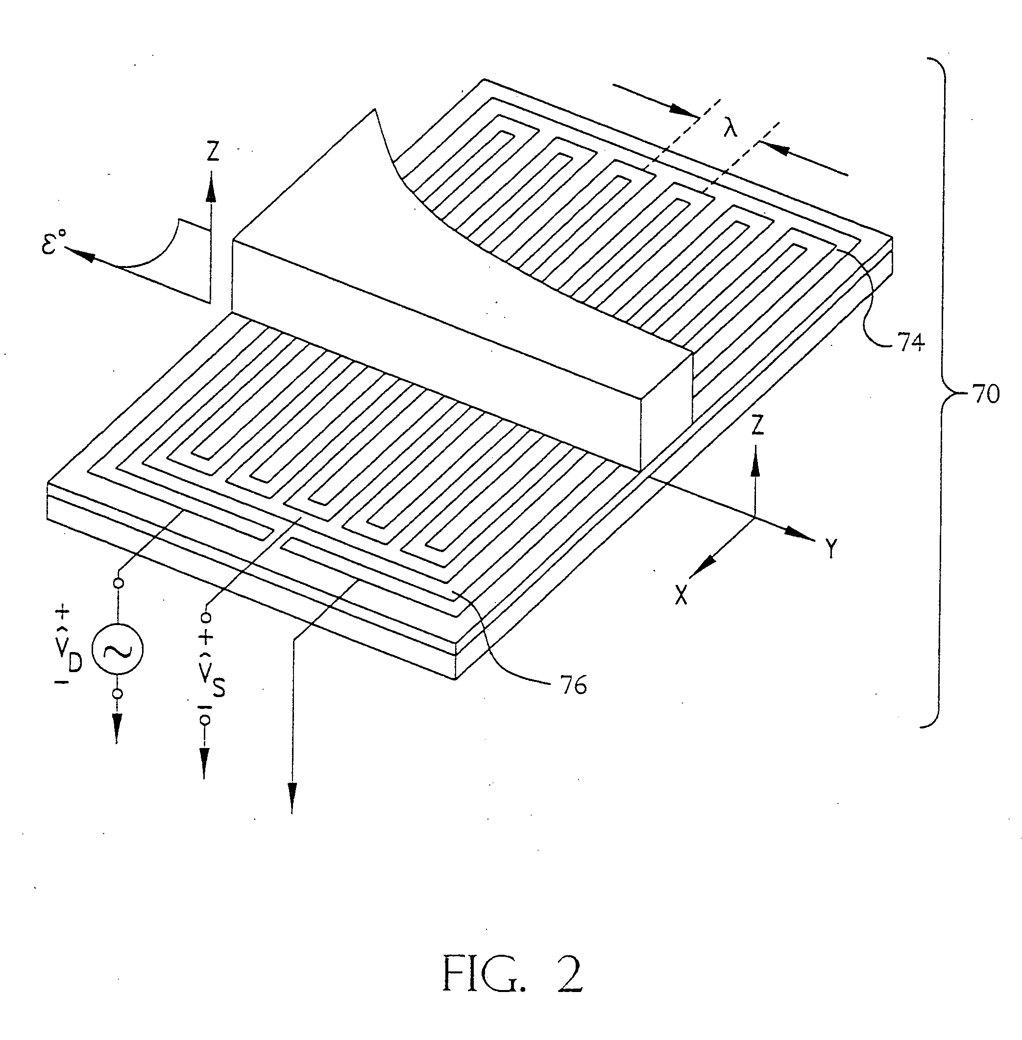
[0041] A measurement apparatus 30 is illustrated in FIG. 1. The measurement apparatus 30 includes an electromagnetic element 32 comprised of voltage driven electrode 34, voltage or current sensing electrode 36, a dielectric substrate 38 that is preferably highly electrically insulating, and a highly conducting back plane 40.

[0042] The driven electrode 34 has an imposed electrical excitation, typically either a voltage or current that can be either periodically varying in time such as sinusoidally or square wave varying with time at frequency f measured in Hertz for frequency dom...


PUM


Abstract

A method is disclosed for processing, optimization, calibration, and display of measured dielectrometry signals. A property estimator is coupled by way of instrumentation to an electrode structure and translates sensed electromagnetic responses into estimates of one or more preselected properties or dimensions of the material, such as dielectric permittivity and ohmic conductivity, layer thickness, or other physical properties that affect dielectric properties, or presence of other lossy dielectric or metallic objects. A dielectrometry sensor is disclosed which can be connected in various ways to have different effective penetration depths of electric fields but with all configurations having the same air-gap, fluid gap, or shim lift-off height, thereby greatly improving the performance of the property estimators by decreasing the number of unknowns. The sensor geometry consist of a periodic structure with, at any one time, a single sensing element that provides for multiple wavelength within the same sensor footprint.

Description

RELATED APPLICATIONS [0001] This application is a continuation of U.S. application Ser. No. 10 / 040,797, filed Jan. 7, 2002, which is a divisional of U.S. application Ser. No. 09 / 310,507, filed May 12, 1999, which claims the benefit of Provisional Application No. 60 / 085,201, filed May 12, 1998, the entire teachings of which are incorporated herein by reference.BACKGROUND OF THE INVENTION [0002] The technical field of this invention is dielectrometry and, in particular, the electromagnetic interrogation of materials of interest to deduce their physical, chemical, geometric, or kinematic properties. The disclosed invention applies to semiconducting, both lossy and lossless dielectric media, very thin metalizations, and shape / proximity measurements for conducting and dielectric objects and surfaces. [0003] Dielectric sensors are commonly used for material property characterization and defect detection in a material under test (MUT). The sensors respond to the absolute properties of the ...

Claims


Application Information

Patent Timeline
IPC IPC(8): G06F19/00G01N27/02G01N27/26G01R27/26
CPCG01R27/2623
Inventor GOLDFINE, NEIL J.ZAHN, MARKUSMAMISHEY, ALEXANDER V.SCHLICKER, DARRELL E.WASHABAUGH, ANDREW P.
Owner GOLDFINE NEIL J
Why Eureka
Try Eureka