Hetero-junction bipolar transistor and manufacturing method of the same

a technology of bipolar transistors and manufacturing methods, applied in the direction of basic electric elements, electrical equipment, semiconductor devices, etc., can solve the problems of thermal runaway and destruction, serious problems may occur, and the high frequency characteristics are degraded, so as to suppress the increase in the chip area and improve the thermal stability and fracture resistance. , the effect of improving the thermal stability and fracture resistan

Inactive Publication Date: 2006-11-30
PANASONIC CORP
View PDF5 Cites 73 Cited by
  • Summary
  • Abstract
  • Description
  • Claims
  • Application Information

AI Technical Summary

Benefits of technology

[0015] In order to solve the problem, an object of the present invention is to improve thermal stability and fr

Problems solved by technology

In the end, the HBT causes thermal runaway and is destroyed.
This phenomenon is more likely to occur as output increases, and a serious problem may occur particularly in HBTs for high-output GSMs.
However, when a ballast resistor is simply placed, high frequ

Method used


Image

  • Hetero-junction bipolar transistor and manufacturing method of the same
  • Hetero-junction bipolar transistor and manufacturing method of the same
  • Hetero-junction bipolar transistor and manufacturing method of the same

Examples


Embodiment Construction

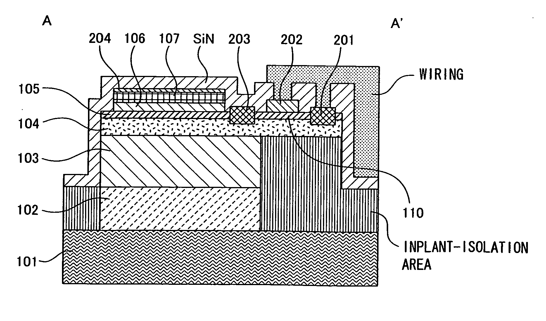
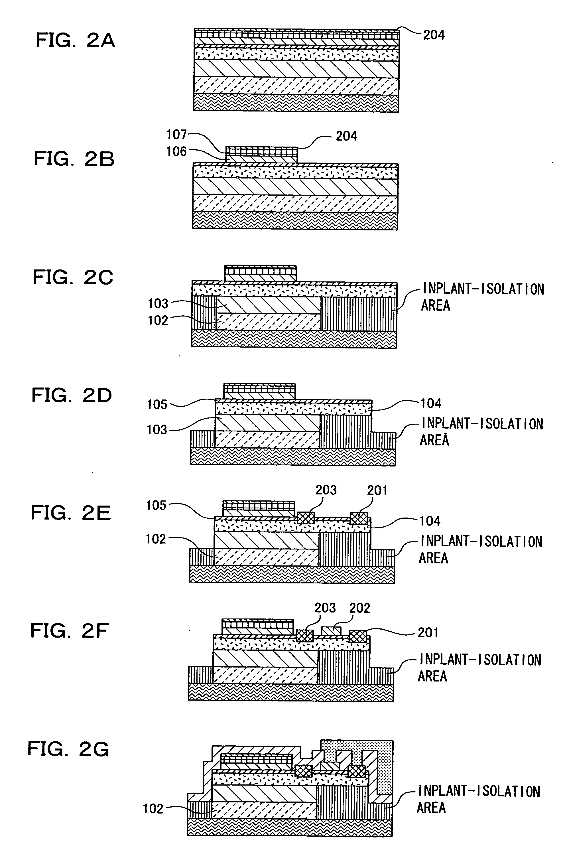
[0034] Referring to FIGS. 1A and 1B and FIGS. 2A to 2G, the following will specifically describe embodiments of a hetero-junction bipolar transistor according to the present invention.

[0035]FIGS. 1A and 1B each is a diagram showing the structure of the hetero-junction bipolar transistor according to the present invention. FIG. 1A is a plan view and FIG. 1B is a cross sectional view taken along line A-A′ of the plan view of FIG. 1A. FIGS. 2A to 2G each is a cross-sectional view showing a process of the manufacturing method of the hetero-junction bipolar transistor according to the present invention. The cross sections are taken at the same position as that of FIG. 1B.

[0036] As shown in FIGS. 1A and 1B, the hetero-junction bipolar transistor is basically configured as follows: an n+ type GaAs sub-collector layer 102 doped with a high-concentration n-type impurity, a 500 nm thick collector layer 103 made of GaAs doped with a low-concentration n-type impurity, a 100 nm thick GaAs base...


PUM


Abstract

Ion implantation is performed on a collector area under an external base area, and a capacitance film is provided on the external base area above the collector area.

Description

FIELD OF THE INVENTION [0001] The present invention relates to a hetero-junction bipolar transistor used as an RF analog device and a manufacturing method of the same. BACKGROUND OF THE INVENTION [0002] Hetero-junction bipolar transistors (HBTs), in which semiconductors with large band gaps are used for emitters, have been put into practical use as RF analog devices for cellular phones and so on. Particularly InGaP / GaAs HBTs using InGaP for emitters are reliable devices with less temperature dependence, and the usage thereof is expected to be wider in the future. [0003] The use of InGaP / GaAs HBTs has expanded in recent years. As to cellular phone transmitter amplifiers, studies have been conducted on the actual use of such HBTs as power devices in the transmission units of GSM terminals as well as conventional CDMA terminals. [0004] When conventional HBTs are used as high power transistors, about 5 to 100 HBTs, each of which acts as a unit cell, are connected in parallel. However, a...

Claims


Application Information

Patent Timeline
IPC IPC(8): H01L31/00
CPCH01L29/41708H01L29/7371H01L29/66318H01L29/42304
Inventor MURAYAMA, KEIICHI
Owner PANASONIC CORP
Why Eureka
Try Eureka