System and method for configuring conductors within an integrated circuit to reduce impedance variation caused by connection bumps

a technology of integrated circuits and configuration methods, applied in the direction of basic electric elements, semiconductor devices, electrical apparatus, etc., can solve the problems of affecting the performance of semiconductor devices, affecting the performance of microelectronic devices, and driving continual shrinkage of microelectronic structures, so as to improve the performance of semiconductor devices, stabilize the power network, and normalize the impedance of metal lines

Inactive Publication Date: 2006-11-30
KK TOSHIBA
View PDF1 Cites 6 Cited by
  • Summary
  • Abstract
  • Description
  • Claims
  • Application Information

AI Technical Summary

Benefits of technology

[0010] A technical advantage of the invention is the ability to stabilize the power network. For example, semiconductor devices using connection-bumps for I/O and power connections may have connection-bumps over the majority of the semiconductor device. However, some constraints prevent arranging connection-bumps in all areas of the semiconductor device. Such areas having a lower density of power bumps generally have bigger power bounce during semiconductor device operation, and such power bounce leads to semiconductor device malfunction.
[0011] This invention provides the ability to normalize metal line impedance in view of semiconductor features or operational characteristics which may influence impedance. Such equalized line impedance may reduce excessive voltage-drop which may

Problems solved by technology

The demand for faster and smaller microelectronic devices is driving continual shrinkage of microelectronic architectures.
However, the connection-bumps which electrically couple a semiconductor de

Method used


Image

  • System and method for configuring conductors within an integrated circuit to reduce impedance variation caused by connection bumps
  • System and method for configuring conductors within an integrated circuit to reduce impedance variation caused by connection bumps
  • System and method for configuring conductors within an integrated circuit to reduce impedance variation caused by connection bumps

Examples


Embodiment Construction

[0022] The invention and the various features and advantageous details thereof are explained more fully with reference to the nonlimiting embodiments that are illustrated in the accompanying drawings and detailed in the following description. Descriptions of well known starting materials, processing techniques, components and equipment are omitted so as not to unnecessarily obscure the invention in detail. It should be understood, however, that the detailed description and the specific examples, while indicating preferred embodiments of the invention, are given by way of illustration only and not by way of limitation. After reading the specification, various substitutions, modifications, additions and rearrangements will become apparent to those skilled in the art from this disclosure which do not depart from the scope of the appended claims.

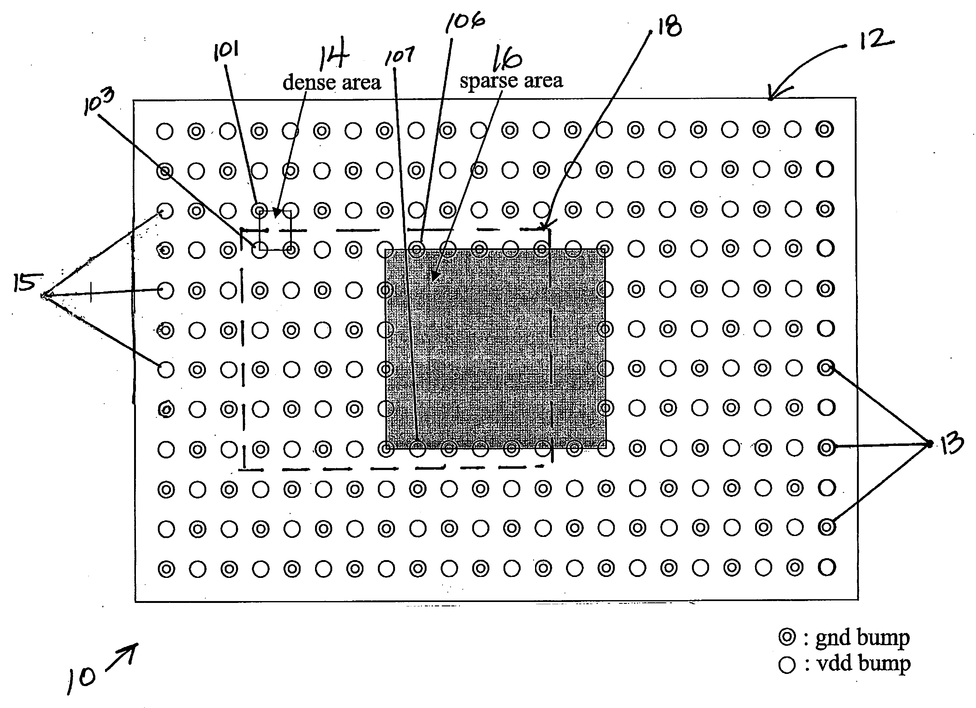
[0023]FIG. 1 is a diagram illustrating one embodiment of a semiconductor device with connection-bumps. Shown in FIG. 1 is a plan view of a sem...


PUM


Abstract

Systems and methods for improved semiconductor device performance are disclosed. In particular, presented are improved semiconductor systems and methods for configuring conductors to reduce impedance variation caused by proximity and/or density and/or operation of connection-bumps. The invention includes adding impedance-reducing conductive features which add no additional functionality to the semiconductor device. The added features may be arranged in areas of sparse connection-bump density. Impedance-reducing conductive features may include metal lines added between functional metal lines, where placement between adjacent functional lines may vary. Impedance-reducing conductive features may be added to any one or combination of conductive layers, and added features may act upon any one or combination of functional features. Further, added features may be electrically active and responsive to semiconductor device operation. Also, methods for determining connection-bump density, which methods may be automated.

Description

TECHNICAL FIELD OF THE INVENTION [0001] The invention relates in general to systems and methods for configuring conductors within an integrated circuit. More specifically, it relates to providing a stable semiconductor device power network by reducing impedance variation within metal power lines caused by connection-bumps on the semiconductor device. BACKGROUND OF THE INVENTION [0002] The demand for faster and smaller microelectronic devices is driving continual shrinkage of microelectronic architectures. Such microelectronic architectures form the electronic circuits of semiconductor devices. Semiconductor devices are manufactured on silicon wafers using a process of adding layers and selectively removing parts of the layers. Semiconductor device features are created through this selective removal process. Upon the completion of the manufacturing process, the silicon wafers are cut into individual dies where each die includes at least one complete semiconductor device. [0003] Indiv...

Claims


Application Information

Patent Timeline
IPC IPC(8): H01P5/02
CPCH01L23/5286H01L23/64H01L2924/3011H01P5/02H01L2924/0002H01L2924/00
Inventor TAKASE, SATORU
Owner KK TOSHIBA
Why Eureka
Try Eureka