Method for driving solid-state imaging device and solid-state imaging device

a technology of imaging element and solid-state imaging, which is applied in the direction of color television details, television systems, radio control devices, etc., can solve the problems of terribly deteriorating image and cause the rise of the minimum driving voltag

Inactive Publication Date: 2006-11-30
FUJIFILM CORP
View PDF8 Cites 3 Cited by
  • Summary
  • Abstract
  • Description
  • Claims
  • Application Information

AI Technical Summary

Benefits of technology

[0029] An object of an illustrative, non-limiting embodiment of the invention is to provide a method for driving a solid-state imaging element and a solid-state imaging device in which even when the length of a reading elect

Problems solved by technology

As a result, a problem arises that a minimum driving voltage is caused to rise.
The remaining sign

Method used


Image

  • Method for driving solid-state imaging device and solid-state imaging device
  • Method for driving solid-state imaging device and solid-state imaging device
  • Method for driving solid-state imaging device and solid-state imaging device

Examples


Embodiment Construction

[0058] Now, an exemplary embodiment of a method for driving a solid-state imaging element and a solid-state imaging device will be described below in detail by referring to the drawings.

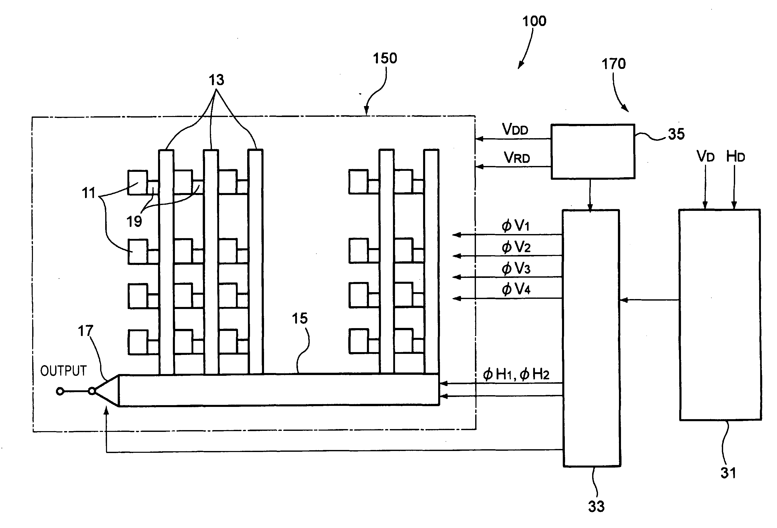
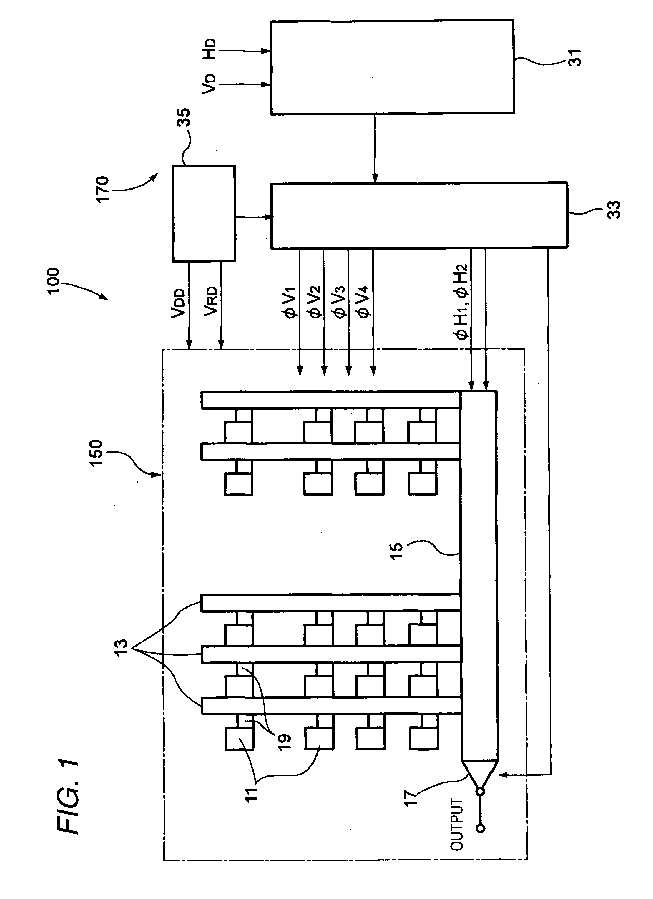
[0059]FIG. 1 shows a schematic block diagram of a solid-state imaging device according to an exemplary embodiment of the present invention.

[0060] The solid-state imaging device 100 includes a solid-state imaging element 150 such as a CCD and an element driving part 170 for inputting a driving signal to the solid-state imaging element 150. The element driving part 170 includes a timing signal generating part 31 for generating various pulse signals for driving the solid-state imaging element 150 in accordance with a horizontal synchronizing signal HD and a vertical synchronizing signal VD, a driver 33 for changing the various pulses supplied from the timing signal generating part 31 to drive pulses of prescribed levels and supplying the drive pulses to the solid-state imaging element 150 and a drivin...


PUM


Abstract

A method for driving a solid-state imaging element, which includes photoelectric conversion parts; vertical charge-transfer paths transferring signal charges from the photoelectric conversion parts in the vertical direction, each of the vertical charge-transfer paths including pairs of a first and second electrodes; and a horizontal charge-transfer path transferring the signal charge in a horizontal direction, is provided and includes applying driving pulses to the first and second electrodes to transfer the signal charge in the vertical direction. The transferring of the signal charge in the vertical charge-transfer paths is performed in such a way that when the signal charge is transferred from an electrode whose length is longer, a charge transfer time is lengthened, and that when the signal charge is transferred from an electrode whose length is shorter, a charge transfer time is shortened.

Description

FIELD OF THE INVENTION [0001] The present invention relates to a method for driving a solid-state imaging element and a solid-state imaging device. BACKGROUND OF THE INVENTION [0002] A structure of a solid-state imaging device is described by referring to FIG. 1. A solid-state imaging device 100 having a solid-state imaging element such as a CCD includes a solid-state imaging element 150 and an element driving part 170 for inputting a driving signal to the solid-state imaging element 150. The solid-state imaging element 150 is driven and controlled in accordance with an output signal from the element driving part 170. [0003] The solid-state imaging element 150 includes a plurality of photodiodes (photoelectric conversion parts) 11 arranged two-dimensionally, a plurality of rows of vertical shift registers (hereinafter, sometimes refer to as vertical charge transfer paths) 13 for reading signal charges generated in the photodiodes 11 in the direction of rows of the arrangement of the...

Claims


Application Information

Patent Timeline
IPC IPC(8): H04N5/335H01L27/148H04N5/357H04N5/369H04N5/372H04N5/376
CPCH04N5/335H04N3/1568H04N25/73H04N25/745
Inventor KOBAYASHIIKEDA, KATSUMI
Owner FUJIFILM CORP
Why Eureka
Try Eureka