Semiconductor memory device and data write and read method thereof

Active Publication Date: 2006-11-30
SAMSUNG ELECTRONICS CO LTD
View PDF8 Cites 22 Cited by
  • Summary
  • Abstract
  • Description
  • Claims
  • Application Information

AI Technical Summary

Benefits of technology

[0006] An embodiment includes a semiconductor memory device including a memory cell array for writing and reading data, a clock signal generating means for receiving an external clock signal applied from an external portion to generate first and second clock signals which have the same phase and frequency as the external clock signal during a normal operation including a normal read operation and a normal write operation and to generate the first clock signal which has the same phase and frequency as the external clock signal and a second clock signal which has the same phase as and a higher frequency than the external clock signal during a test operation including a test read operation and a test write operation, a data write means for receiving a first predetermined-bit serial data applied at a first data rate and converting the first predetermined-bit serial data into a first predetermined-bit parallel data to be outputted to the memory cell array during the normal write operation and for receiving a second predetermined-bit serial data applied at the first data rate and converting the second predetermined-bit serial data into parallel data to be outputted to the memory cell array during the test write operation, and a data read means for generating a predetermined-bit parallel data outputted from the memory cell array in response to the first clock signal during the normal and test operations, converting the predetermined-bit parallel data into serial data and outputting the serial data at the first data rate in response to the second clock signal during the normal read operation, and converting the predetermined-bit parallel data into serial data and outputting the serial data at the second data rate in response to the second clock signal during the test read operation.
[0007] A further embodiment includes a semiconductor memory device including an address input means for receiving and buffering an address which are sequentially applied at least twice in response to a rising edge of an external clock signal applied from an external portion during a normal operation including a normal read operation and a normal write operation and for receiving and buffering an address which is sequentially applied at least twice in response to rising and falling edges of the external clock signal during a test operation including a test read operation and a test write operation, a memory cell array for writing and reading data in at least one cell which the address designates, a clock signal generating means for receiving the external clock signal to generate first and second clock signals which have the same phase and frequency as the external clock signal during the normal operation and to generate the first clock signal which has the same phase and frequency as the external clock signal and a second clock signal which has the same phase as and a higher frequency than the external clock signal during

Problems solved by technology

An expensive test device is necessary to test a semiconductor memory device that may operate at a high frequency, specifically a device that may operate with a clock signal having a frequency in excess of 1 GHz.
Such an expensive test device may be capable of generating a clock signal having a frequency greater than 1 GHz.
Less expensive test devices may not be able to gener

Method used


Image

  • Semiconductor memory device and data write and read method thereof
  • Semiconductor memory device and data write and read method thereof
  • Semiconductor memory device and data write and read method thereof

Examples


Example

[0022] Embodiments will now be described more fully hereinafter with reference to the accompanying drawings. Embodiments may take different forms and should not be construed as limited to the embodiments set forth herein. Rather, these embodiments are provided so that this disclosure will be thorough and complete, and will fully convey the scope to those skilled in the art.

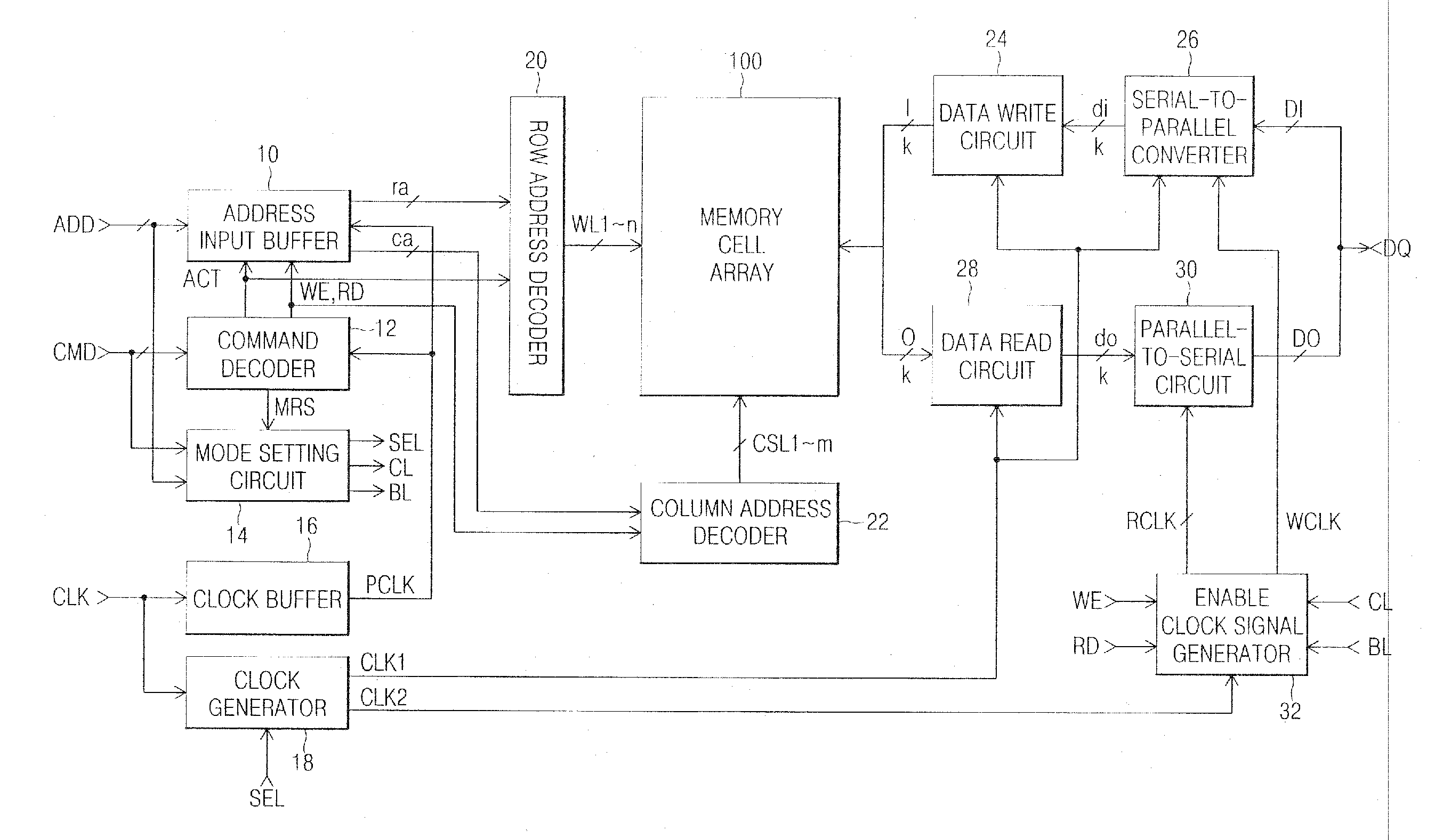
[0023]FIG. 1 is a block diagram illustrating a semiconductor memory device. The semiconductor memory device of FIG. 1 includes a memory cell array 100, an address input buffer 10, a command decoder 12, a mode setting circuit 14, a clock buffer 16, a clock generator 18, a row address decoder 20, a column address decoder 22, a data write circuit 24, a serial-to-parallel converter 26, a data read circuit 28, a parallel-to-serial converter 30, and an enable clock signal generator 32.

[0024] Functions of the components of FIG. 1 are explained below.

[0025] The address input buffer 10 receives and buffers an address AD...


PUM


Abstract

A semiconductor memory device includes a serial to parallel converter configured to generate parallel data at a parallel data rate in response to first serial data at first serial data rate in a first mode and configured to generate the parallel data at the parallel data rate in response to a second serial data at second serial data rate in a second mode, wherein the second serial data rate is less than the first serial data rate, and a data write circuit configured to provide the parallel data to a memory cell array.

Description

CROSS-REFERENCE TO RELATED APPLICATION[0001] This application claims the benefit of Korean Patent Application No. 2005-43754, filed May 24, 2005, the disclosure of which is hereby incorporated herein by reference in its entirety. BACKGROUND [0002] 1. Technical Field [0003] This disclosure relates to a semiconductor memory device and, more particularly, to a semiconductor memory device and data write and read method thereof which operates at a high frequency. [0004] 2. Description of the Related Art [0005] An expensive test device is necessary to test a semiconductor memory device that may operate at a high frequency, specifically a device that may operate with a clock signal having a frequency in excess of 1 GHz. Such an expensive test device may be capable of generating a clock signal having a frequency greater than 1 GHz. Less expensive test devices may not be able to generate a clock signal having as high a frequency but may be able to receive data output from the semiconductor m...

Claims


Application Information

Patent Timeline
IPC IPC(8): G11C7/10
CPCG11C29/12015G11C29/32G11C29/14G11C7/22G11C29/00
Inventor JANG, SEONG-JIN
Owner SAMSUNG ELECTRONICS CO LTD
Why Eureka
Try Eureka