Chip information managing method, chip information managing system, and chip information managing program

Active Publication Date: 2006-11-30
MICRON TECH INC
View PDF1 Cites 7 Cited by
  • Summary
  • Abstract
  • Description
  • Claims
  • Application Information

AI Technical Summary

Benefits of technology

[0022] According to one aspect of the present invention, there are provided a chip information managing method, a chip information managing system, and a chip information managing program, which make it possible to store desired information on a semiconductor chip, by only referring to a data table that allocates information to a relationship between defective addresses and a defective address storing circuit that stores these defective addresses.
[00

Problems solved by technology

There are many complex factors that degrade productivity, and it is not always easy to pinpoint these factors.
However, in a wafer state before a semiconductor wafer is divided into semiconductor chips, there are characteristics in positions where defects occur, depending on factors that degrade productivity of chips.
However, while it is relatively easy to specify a position of the occurrence of a defect in the wafer state before division into chips, it is considerably difficult to specify this position after the wafer is divided into individual chips by dicing.
This results in increasing the manufacturing cost of chips.
Semiconductor chips that are normal in the state before dicing will also become defective after the dicing.
In this case, it is substantially impossible to obtain information concerning a position of the occurrence of the defect on the wafer.
Ho

Method used


Image

  • Chip information managing method, chip information managing system, and chip information managing program
  • Chip information managing method, chip information managing system, and chip information managing program
  • Chip information managing method, chip information managing system, and chip information managing program

Examples


Embodiment Construction

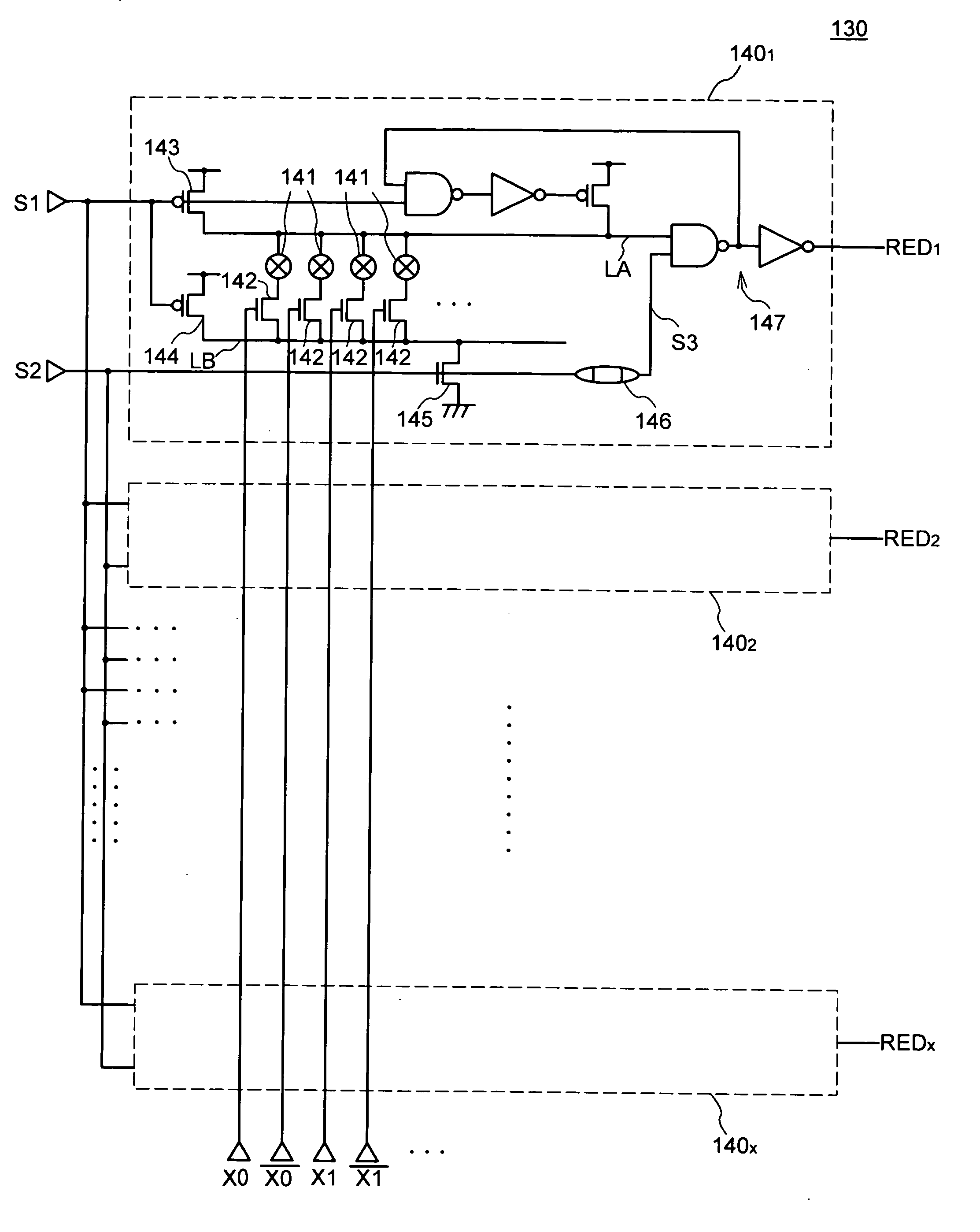
[0047] Before explaining in detail preferred embodiments of the present invention, an outline configuration of a semiconductor chip to which the invention can be applied and principle of the invention are explained below.

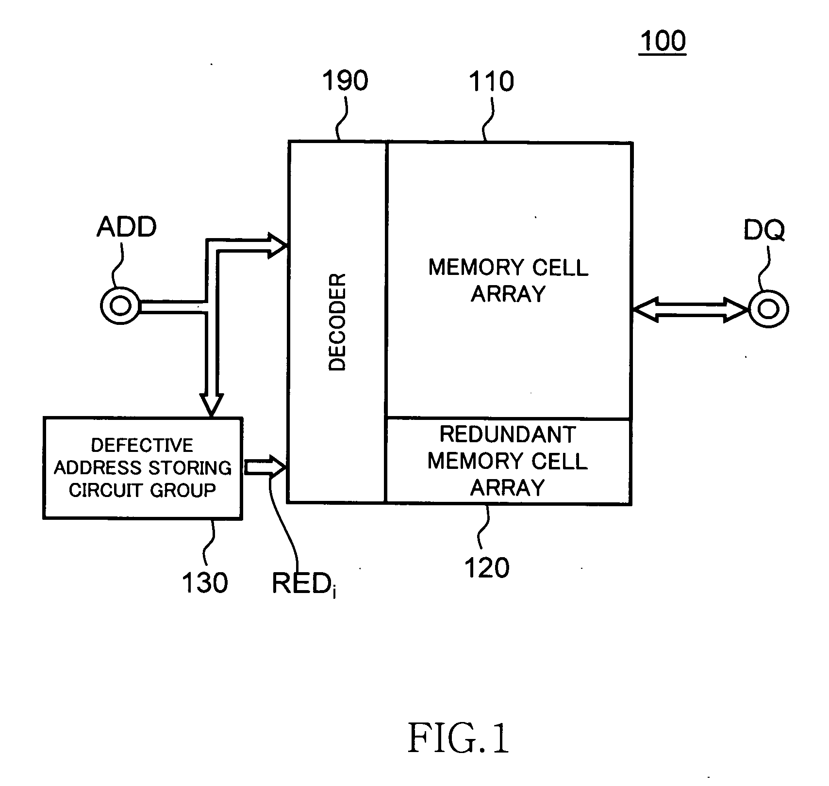
[0048]FIG. 1 is a block diagram showing key elements of a semiconductor chip to which the present invention can be applied.

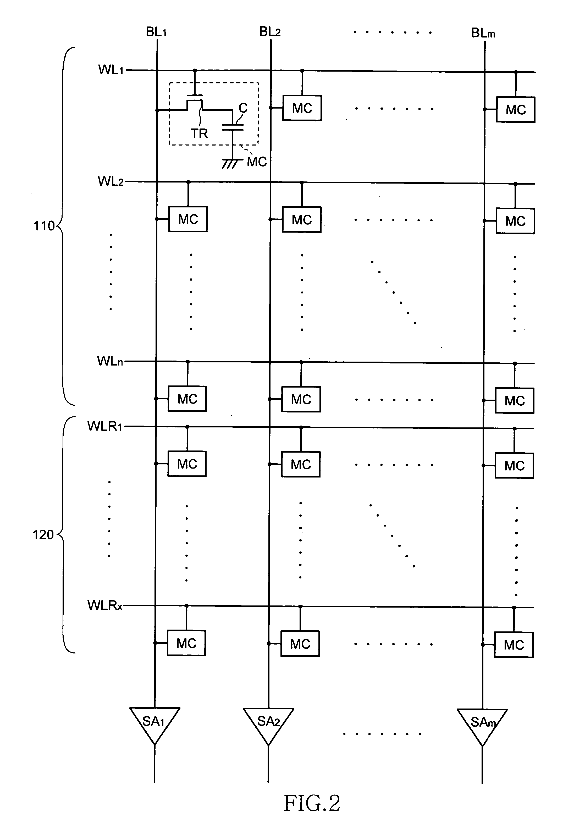
[0049] As shown in FIG. 1, a semiconductor chip 100 to which the present invention can be applied includes at least: a memory cell array 110 including plural memory cells; a redundant memory cell array 120 that saves defective addresses; a defective address storing circuit group 130 that stores defective addresses; and a decoder 190 that accesses the memory cell array 110 and the redundant memory cell array 120.

[0050] This semiconductor chip 100 can be a DRAM and a memory-logic integrated chip. The semiconductor chip 100 has a function of accessing a predetermined memory cell included in the memory cell array 110, based on an address signal s...


PUM


Abstract

In replacing word lines having defective addresses with redundant word lines, information is held in a relationship between the word lines and the redundant word lines. In other words, information is held in a replacement rule. With this arrangement, information such as a lot number, a wafer number within the lot, and a position of a chip within the wafer can be held in the chip, without increasing the chip area at all and without using a large database.

Description

TECHNICAL FIELD [0001] The present invention relates to a chip information managing method, a chip information managing system, and a chip information managing program. Particularly, the present invention relates to a chip information managing method, a chip information managing system, and a chip information managing program, of a semiconductor chip having a redundant memory cell array to save a defective address. BACKGROUND OF THE INVENTION [0002] A semiconductor chip such as a DRAM (Dynamic Random Access Memory) is manufactured in a wafer unit by diffusion processing in a front-end process. A semiconductor wafer obtained in the front-end process is divided to produce many semiconductor chips in a post-process, as is well known. Therefore, in order to manufacture one semiconductor chip at lower cost, it is important to increase the number of semiconductor chips obtained from one semiconductor wafer and to improve productivity of the semiconductor chips obtained. [0003] The increas...

Claims


Application Information

Patent Timeline
IPC IPC(8): G11C29/00
CPCG11C11/401G11C2029/4402G11C29/838G11C29/783
Inventor OGAWA, SUMIO
Owner MICRON TECH INC
Why Eureka
Try Eureka