

CMOS type image sensor module having transparent polymeric encapsulation material
a polymer encapsulation material and image sensor technology, applied in the field of image pick-up devices, can solve the problems of frequent manufacturing defects, high production cost, and disadvantages of the above-described cmos type of image sensor modules, and achieve the effect of simple process
- Summary
- Abstract
- Description
- Claims
- Application Information
AI Technical Summary
Benefits of technology
Problems solved by technology
Method used
Image

Examples
first embodiment
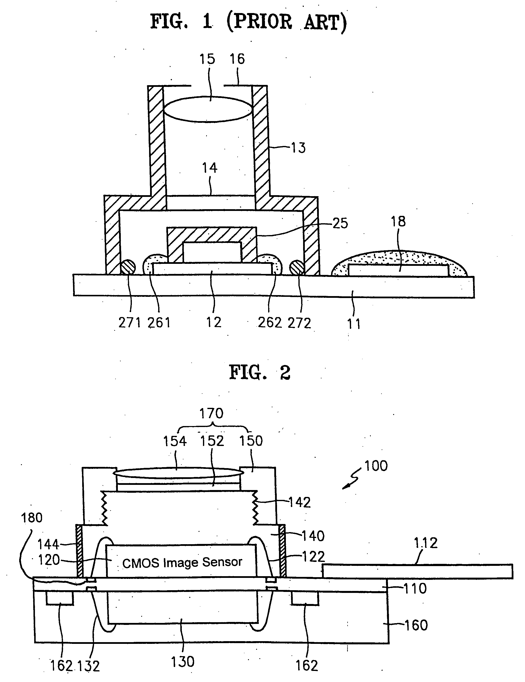
[0027] Referring to FIG. 2, CMOS type of image sensor module 100 according to the present invention includes a substrate 110 having a circuit pattern to which a chip can be wire bonded at either side thereof, a first semiconductor chip (image sensing chip having a CMOS type of image sensor) 120 mounted on an upper portion of the substrate 110 and wire-bonded to the circuit pattern thereof, a second semiconductor chip (digital signal processing chip) 130 mounted on a lower portion of the substrate 110 and wire-bonded to the circuit pattern thereof, and a sealing resin unit 140 of transparent polymeric encapsulation material formed on the surface of the substrate 110 by injection molding and in which the first semiconductor chip 120 is sealed.
[0028] The CMOS type of image sensor module 100 further includes an epoxy molding compound 160 on the lower portion of the substrate 110 and in which a passive device 162 and the second semiconductor chip 130 are sealed, protective material 144 a...
third embodiment
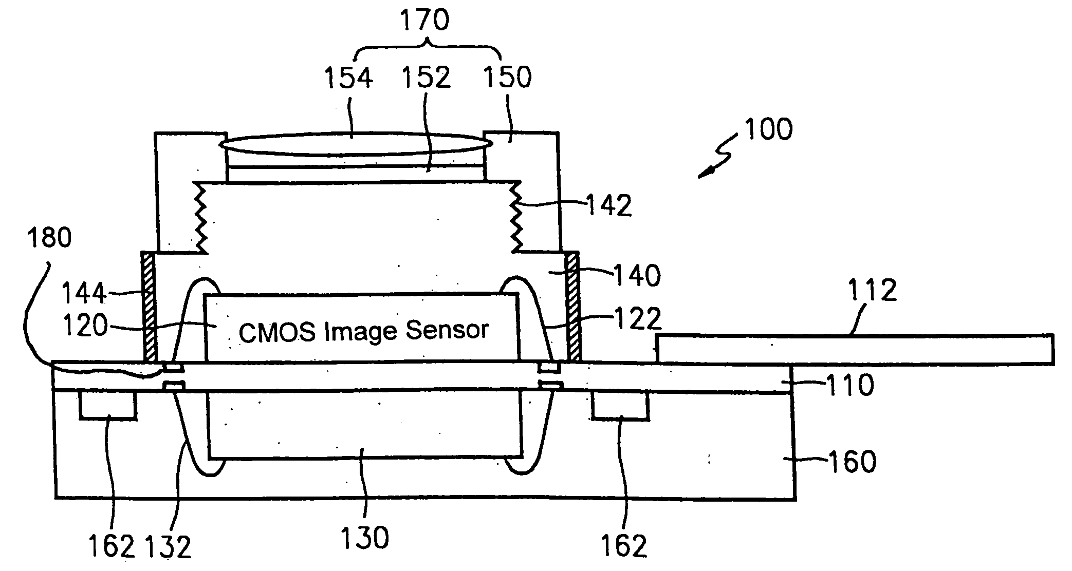
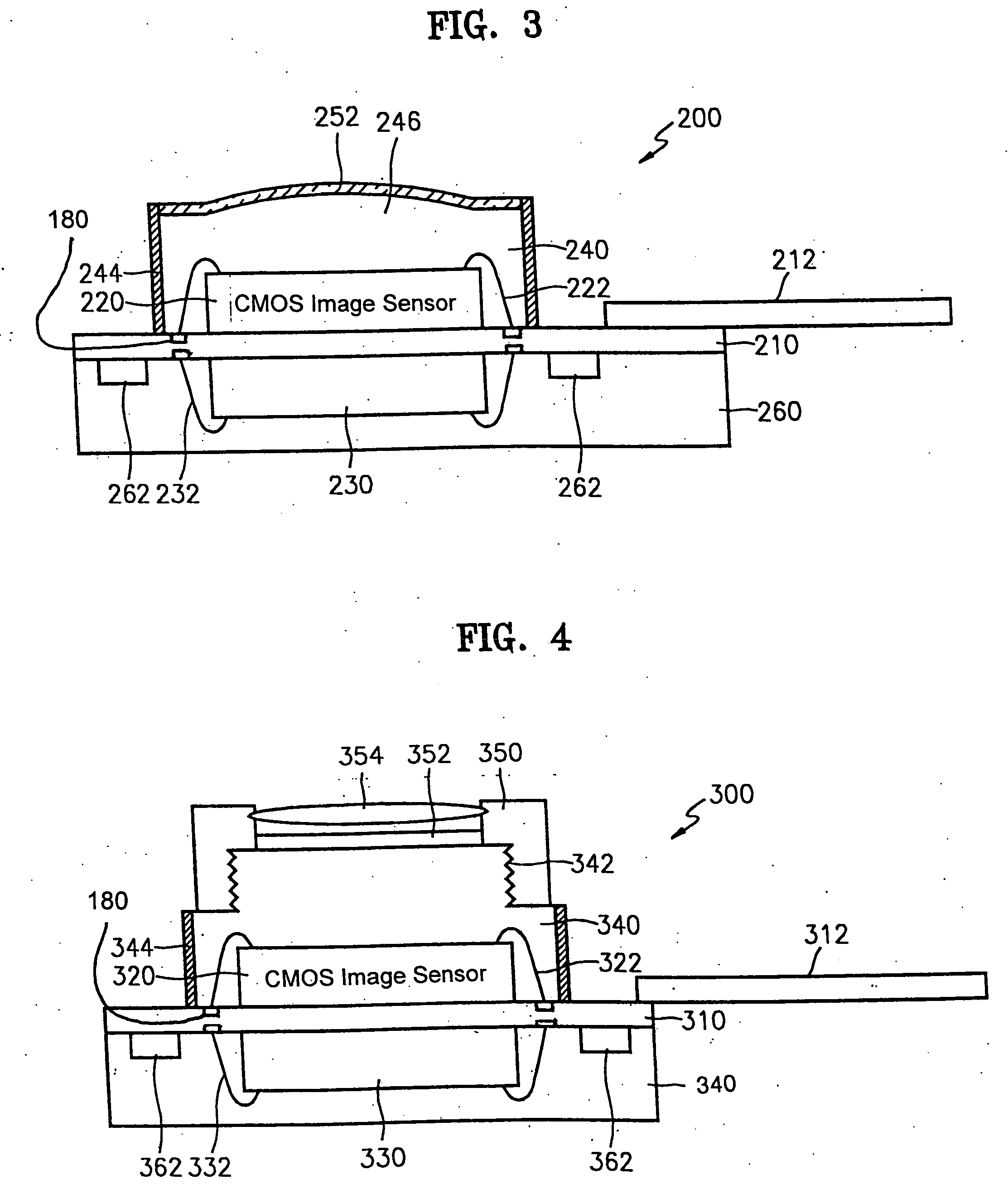
[0039] a CMOS type of image sensor module according to the present invention will now be described with reference to FIG. 4.
[0040] In this embodiment, a sealing resin unit 340 is formed on both the upper and lower portion of a substrate 310, i.e., an epoxy compound is not molded to the lower portion of the substrate 310. The remaining parts are identical to those of the embodiment of FIG. 2. For instance, the sealing resin unit 340 has a screw thread 342, and a lens kit is threaded to the sealing resin unit 342. The lens kit includes a lens housing 350, an infrared filter 352, and an optical lens 354. Reference numerals 322, 332 designate bonding wires, 362 a passive device, and 312 a flexible printed circuit board (FPCB).
fourth embodiment
[0041] a CMOS type of image sensor module according to the present invention will now be described with reference to FIG. 5.
[0042] This embodiment is the same as the third embodiment in that a sealing resin unit 440 is formed on both the upper and lower portions of the substrate 410, i.e., an epoxy compound is not molded to the lower portion of the substrate 410. In this embodiment, though, like the second embodiment of FIG. 3, an optical lens 446 is formed by the upper portion of the sealing resin unit 440, and the plastic lens 446 is coated with an infrared filter 452. Reference numerals 422, 432 designate bonding wires, 462 a passive device, and 412 a flexible printed circuit board (FPCB).
[0043] Methods of manufacturing CMOS type of image sensor modules 300 and 400 according to the present invention will be described below.
[0044] First, a substrate 310, 410 including a circuit pattern at both sides thereof is prepared. The doubled-sided substrate 310, 410 is similar to that of ...
PUM
 Abstract
Description
Claims
Application Information