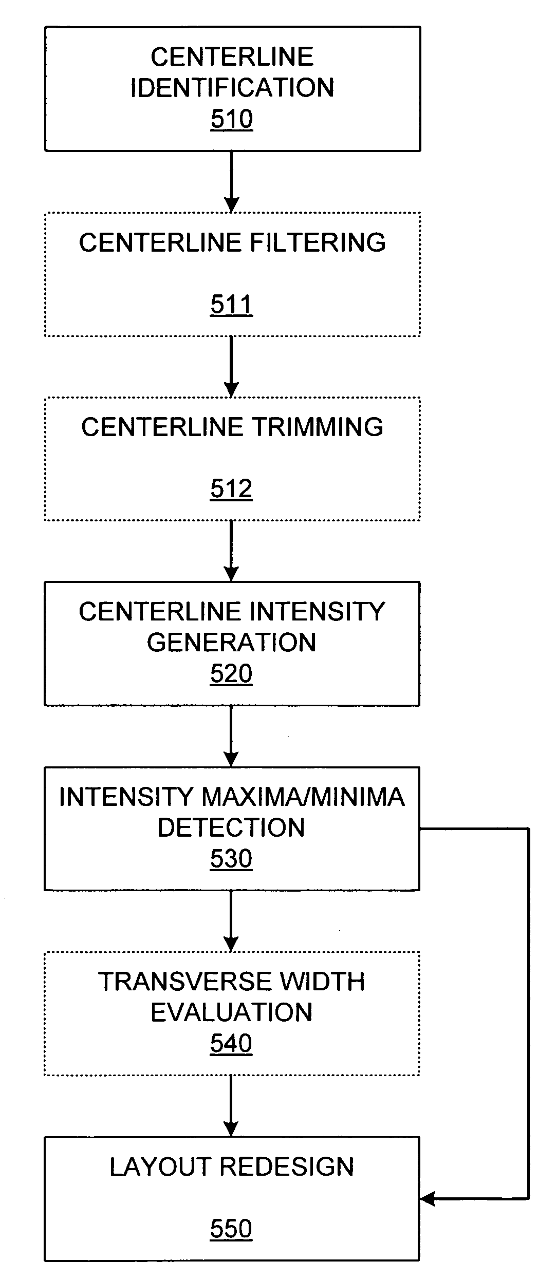
[0043] Modern IC designs have evolved beyond the capabilities of physical verification, and now generally require some sort of simulation-based verification to detect potential defect-inducing layout configurations. However, conventional simulation-based verification, which can provide accurate detection of portions of a mask layout likely to generate pinch/bridge defects, can also be too computationally expensive to perform efficient layout checking.
[0044] By applying a centerline intensity-based layout verification technique, even the most complex and dense IC layouts can be quickly and accurately evaluated for defect-inducing regions. Specifically, by performing lithography simulation only along selected centerlines and check positions of a mask layout, the defect detection benefits of simulation-based verification can be achieved at a much lower computational cost.
[0045]FIG. 4A shows an embodiment of a computer system 400 that can perform layout verification based on centerline intensity data. Computer system 400 includes a graphical display unit 410 (e.g., a computer monitor) and a processing unit 420 (e.g., a personal computer). Note that any graphical representations depicted on graphical display unit 410 in FIGS. 4A and 4B are purely for explanatory purposes, and that in various other embodiments, graphical display unit 410 can display any type or manner of graphical representation of the processes described with respect to FIGS. 4A and 4B. Note further that in another embodiment, graphical display unit 410 may be eliminated from the process entirely.
[0046] Processing unit 420 includes centerline definition logic 421, centerline intensity generation logic 422, maxima/minima detection logic 423, and optional transverse width (TW) determination logic 424. In one embodiment, logic 421-424 can comprise a software program (computer instructions) encoded on a computer-readable medium (e.g., hard drive, TW-ROM, or DVD-ROM). In various embodiments, the computer-readable medium can be incorporated into processing unit 420. In various other embodiments, the computer-readable medium can be external to processing unit 420 (e.g., processing unit 420 can be a “thin client” that runs the software from a networked server).
[0047] To begin a verification operation, centerline definition logic 421 identifies the centerlines of mask layout features (i.e., mask layout elements and spaces between mask layout elements) and selects appropriate ones of those centerlines for subsequent evaluation. For example, graphical display unit 410 depicts a mask layout 320 (described above with respect to FIG. 3A) that includes mask layout elements ME1, ME2, ME3, and ME4. Centerline definition logic 421 can identify the centerline(s) of the features in mask layout 320—i.e., the centerlines of each of layout elements ME1-ME4 (i.e., “element centerlines”) and the centerlines of the spaces between adjacent layout elements (i.e., “space centerlines”).
[0048] In one embodiment, centerline definition logic 421 can pass all feature centerlines to centerline intensity generation logic 422 to continue the layout verification process. However, in another embodiment, centerline definition logic 421 can apply filtering rules to the set of all feature centerlines to eliminate from subsequent processing those feature centerlines that are unlikely to be associated with lithography defects. For example, since pinch defects are unlikely to be caused by mask layout elements that are wider than a certain threshold width (e.g., layout element ME4), centerline definition logic 421 could incorporate a filtering rule to ignore the centerlines for such layout elements (or portions of layout elements). Similarly, since a relatively large distance between adjacent mask layout elements (e.g., between layout elements ME3 and ME4) generally means that there will be little chance of bridge defect generation, centerline definition logic 421 could incorporate another filtering rule to ignore centerlines for spacing features greater than a threshold distance. Another filtering rule could be to ignore centerlines from layout elements that are widely spaced from any adjacent layout elements (e.g., layout element ME1). Yet another filtering rule could be to ignore centerlines for spacings between adjacent layout elements that have relatively short facing edge length (e.g., between layout elements ME2 and ME3)—this rule can be restated as ignoring centerlines for spacings having a relatively short length. Various other filtering rules will be readily apparent.
[0049] In another embodiment, the centerlines detected by centerline definition logic 421 can be modified to minimize the risk of false defect detection due to line shortening and corner rounding. Line shortening and corner rounding are common lithographic effects. Line shortening occurs when a relatively long and narrow mask element (a “line element”) is projected onto a wafer and the exposure pattern element corresponding to the line element exhibits shortened line ends. Likewise, when mask layout elements having sharp corners are projected onto a wafer, the corners of the resulting exposure pattern elements typically exhibit some degree of rounding. Depending on the severity of the line shortening and/or corner rounding, such effects can lead to false positives in subsequent defect detection analysis (e.g., the shortened end of an exposure element may be misinterpreted as a pinch defect).
[0050] Therefore, in one embodiment, centerline definition logic 421 can trim a centerline such as centerline CL1 away from the end of any line element (e.g., by a distance T1) and/or from any corner (e.g., by a distance T2). Distances T1 (for line end trimming) and T2 (for corner trimming) would typically be determined based on the model data for the lithography process in which mask layout 320 is to be used, since different lithography processes will generally exhibit different degrees of line shortening and corner rounding. In one embodiment, distances T1 and T2 could be constant trim values for a particular layout design. In another embodiment, trim distances T1 and T2 could be specific to the particular centerline being trimmed (i.e., different centerlines will be trimmed by different amounts, depending on the particular layout details and process characteristics). Note that trimming can be applied to centerlines for both element centerlines and space centerlines.
[0051] Thus, as shown in FIG. 4A, after centerline filtering and/or trimming, centerline definition logic 421 might provide only centerlines CL1 and CL2 to centerline intensity generation logic 422. Centerline intensity generation logic 422 can then perform lithography simulation over centerlines CL1 and CL2 to generate centerline intensity distributions IN1 and IN2 (intensity vs. position). The lithography simulation performed by centerline intensity generation logic 422 is substantially similar to that performed by conventional simulation-based verification tools, except that centerline intensity generation logic 422 only calculates intensity in the portions of the exposure pattern that correspond to the centerlines selected by centerline definition logic 421. Therefore, centerline intensity generation logic can generate centerline intensity distributions IN1 and IN2 very quickly.
[0052] As noted above, lithography simulations generally involve generating a model exposure pattern that is expected to be produced by the mask layout during a lithography operation. The simulated exposure pattern is determined from the mask layout and on model data for a particular process (model data is typically provided by the fab that will be performing the actual lithography operation). The exposure pattern represents the pattern of light (exposure radiation) transmitted by a mask patterned with the mask layout onto a wafer. Due to optical effects (mainly refraction) as the light passes through the mask layout, the light incident on the wafer will exhibit intensity variations, as indicated by the varying profiles of centerline intensity distributions IN1 and IN2.
[0053] Maxima/minima detection logic 423 therefore can evaluate intensity distribution IN1 and IN2 to detect local maxima (e.g., point MAX1 in distribution IN1) and/or local minima (e.g., points MIN1 and MIN2 in distribution IN2). A local maximum in the intensity distribution represents a location on the wafer receiving “greater exposure” than its surroundings, while a local minimum represents a location receiving less exposure than its surroundings. Therefore, the local maxima and minima in the intensity graphs indicate potential pinch/bridge defects in the exposure pattern.
[0054] For example, if mask layout 320 is incorporated into a bright field mask, the intensity of the exposure pattern along centerline CL1 of layout element ME2 would be expected to be a relatively constant low value, since layout element ME2 would be expected to block most of the exposure radiation from reaching the wafer. However, local maximum MAX1 in intensity distribution IN1 indicates that (within the exposure pattern) check position CP1 along centerline CL1 is receiving more light than its neighboring points along centerline CL1. Therefore, check position CP1 represents a potential defect generation location in mask layout 320 (i.e., a location that may generate a (pinch) defect during actual lithography processes).
[0055] At the same time, the intensity of the exposure pattern along centerline CL2 between layout elements ME2 and ME4 would be expected to be a relatively constant high value, since the bright field between layout elements ME2 and ME4 would be expected to transmit most of the exposure radiation onto the wafer. However, local minima MIN1 and MIN2 in intensity distribution IN2 indicate that (within the exposure pattern) check positions CP2 and CP3 along centerline CL2 are receiving less light than their neighboring points along centerline CL2. Therefore, check positions CP2 and CP3 may also represent potential defect generation locations in mask layout 320 (i.e., locations that may generate bridge defects in the resulting exposure pattern).
[0056] Once the check positions (i.e., CP1, CP2, and CP3) in mask layout 320 are identified by maxima/minima detection logic 423, appropriate modifications can be made to mask layout 320 to minimize the chances of defect generation. However, it may be that not all of the check positions correspond to actual pinch or bridge defects (e.g., the pinching produced at location CP1 could be minimal enough to not cause any problems in the final IC). Therefore, to minimize unnecessary layout modification, processing unit 420 can include optional transverse width (TW) determination logic 424 for performing a more in-depth evaluation of the check positions detected by minima/maxima detection logic 423.
[0057] TW determination logic 424 performs localized lithography simulation at the check positions to provide a more detailed view of the actual lithographic behavior in those regions, thereby allowing a determination to be made as to whether defects will actually be generated at each check position. For example, FIG. 4B shows TW determination logic 424 in verification system 400 performing lithography simulation at check positions CP1, CP2, and CP3. For reference purposes, the entire simulation layout 340 (described with respect to FIG. 3B) is shaded and overlaid over mask layout 320 in FIG. 4B. However, TW determination logic 424 only models the portions of projected layout 340 that determine the transverse widths at check positions CP1, CP2, and CP3. Specifically, for each of check positions CP1 through CP3, TW determination logic 424 models the transverse width of the exposure pattern at that particular check position. The transverse width at a given check position is the width perpendicular to the centerline of the exposure pattern feature (i.e., exposure pattern element or space between exposure pattern elements) associated with that check position.
[0058] For example, TW determination logic 424 can perform a lithography simulation to calculate a transverse width TW1 for simulation layout element SE1 at check position CP1. If transverse width TW1 is less than a predetermined pinch threshold value, then a redesign of mask layout 320 in the region of check position CP1 can be performed to avoid generation of pinch defects during actual lithography processes. However, if transverse width TW1 is greater than the pinch threshold value, then no redesign of mask layout 320 is required, since the thinning of simulation element SE2 does not rise to the level of an actual pinch defect. Note that a single pinch threshold value can be used for pinch defect evaluation over an entire layout, or a variety of pinch threshold values can be defined so that different pinch threshold values can be used for different regions in a design (e.g., speed-critical lines may have larger pinch threshold values).
[0059] Similarly, TW determination logic 424 can perform lithography simulation to calculate transverse widths TW2 and TW3 at check positions CP2 and CP3, respectively, for the spacing between simulation elements SE2 and SE4. If transverse widths TW2 and/or TW3 are less than a predetermined bridge threshold value, then a redesign of mask layout 320 in the region(s) of check positions CP2 and/or CP3, respectively, can be performed to avoid generation of bridge defects during actual lithography processes. However, if transverse widths TW2 and TW3 are greater than the bridge threshold value, then no redesign of mask layout 320 is required, since the spacing reductions between simulation elements SE2 and SE4 do not rise to the level of actual bridge defects. Note that a single bridge threshold value can be used for bridge defect evaluation over an entire layout, or a variety of bridge threshold values can be defined so that different bridge threshold values can be used for different regions in a design.
[0060] Thus, by actually calculating the transverse widths at the check positions, an explicit determination can be made of whether or not a pinch or bridge defect is likely to be generated by those locations in the mask layout. By filtering out those check positions that will not actually cause pinch or bridge defects during actual lithography, the amount of subsequent layout redesign can be minimized. Note that because the lithography simulation used to determine the transverse widths is only performed at the check positions, the modeling calculations can be performed very quickly (as opposed to the lengthy computation times required by conventional “full mask” lithography modeling).
[0061]FIG. 5 shows a flow diagram of the layout verification process described with respect to FIGS. 4A and 4B. In a “CENTERLINE IDENTIFICATION” step 510, the element and space centerlines in a layout are identified. In an optional (as indicated by the dotted line) “CENTERLINE FILTERING” step 511, the detected centerlines can be filtered to eliminate those centerlines that are unlikely to be associated with pinch or bridge defects. In an optional “CENTERLINE TRIMMING” step 512, the selected centerlines can be trimmed away from any edges and/or corners in the layout. Note that in one embodiment, step 510, and optionally steps 511 and/or 512, can be performed by centerline definition logic 421 in FIG. 4A.
[0062] Next, in a “CENTERLINE INTENSITY GENERATION” step 520, the expected exposure intensity distributions associated with the previously identified (and filtered/trimmed, if applicable) centerlines are calculated (e.g., by centerline intensity detection logic 422 in FIG. 4A). As noted above, any lithography simulation engine will be able to provide exposure intensity information, and since the intensity data is only required for simulation layout locations associated with element and space centerlines, the intensity data determination can be performed very rapidly using minimal computing resources.
[0063] Then, in an “INTESITY MAXIMA/MINIMA DETECTION” step 530, local maxima and/or minima in the previously determined centerline intensity distributions are identified (e.g., by maxima/minima detection logic 423 in FIG. 4A). Specifically, any peaks or valleys in the intensity distributions are located and evaluated, with each peak/valley defining a check position in the mask layout that represents a potential defect generation location. At this point, the process can go straight to a “LAYOUT REDESIGN” step to adjust those portions of the mask layout that are associated with the centerline intensity maxima/minima detected during step 530. Note that the layout redesign of step 550 will typically be performed outside of the layout verification system. For example, check positions identified by layout verification system 400 in FIG. 4A could be provided to a separate workstation using a separate layout design tool(s) for design modification.
[0064] As noted above with respect to FIGS. 4A and 4B, the centerline intensity peaks/valleys do not definitively indicate locations at which pinch or bridge defects will be generated. Notably, some check positions may turn out to produce exposure patterns that fall within the design specifications. Therefore, in an optional “TRANSVERSE WIDTH EVALUATION” step 540, the transverse width (i.e., the transverse width) of the exposure pattern feature (i.e., an exposure pattern element or a space between exposure pattern elements) associated with each check position is calculated (e.g., by TW determination logic 424 in FIG. 4B). Any check position having a transverse width that is greater than a defect threshold value is removed from the set of locations requiring redesign, thereby minimizing the amount of layout modification required (i.e., only those check positions exhibiting transverse widths less than the defect threshold value require layout redesign). Note that the transverse width determination of step 540 can be performed using the same type of lithography simulation used in conventional simulation-based verification. Because the modeling of step 540 is only performed for a small proportion of the layout (i.e., only at centerline intensity maxima/minima locations), the simulation can advantageously be performed in much less time than is required by conventional “whole layout” simulations.
[0065] Thus, by actually modeling the exposure pattern at the centerline intensity maxima/minima locations, a determination can be made as to which of those locations will probably exhibit pinch/bridge defects, and consequently, which of the associated locations in the mask layout may require redesign. Note that the centerline intensity-based layout verification described with respect to FIG. 5 can be performed at any stage in an IC design process. For example, in one embodiment, the verification can be performed immediately after layout extraction (e.g., after step E124 in FIG. 1). In another embodiment, centerline intensity-based layout verification can be performed after the incorporation of assist features or after the application of OPC (e.g., after step E128 in FIG. 1). Note further that the centerline intensity-based layout verification described with respect to FIG. 5 can be applied to any type of layout (e.g., to a phase shift mask (PSM) layout).
[0066] The various embodiments of the structures and methods of this invention that are described above are illustrative only of the principles of this invention and are not intended to limit the scope of the invention to the particular embodiments described. Thus, the invention is limited only by the following claims and their equivalents.