Wiring board and manufacturing method of wiring board

Active Publication Date: 2006-12-07
NGK SPARK PLUG CO LTD
View PDF17 Cites 56 Cited by
  • Summary
  • Abstract
  • Description
  • Claims
  • Application Information

AI Technical Summary

Benefits of technology

[0016] This configuration makes it possible to form the lowest resin insulating layer with a material that is smaller than the adjacent resin insulating layer in the linear expansion coefficient. In particular, the lowest resin insulating layer can be made of a material whose linear expansion coefficient lies halfway between the linear expansion coefficients of the adjacent resin insulating layer and the ceramic sub-core, which provides an effect of absorbing a difference in the linear expansion coefficient in the thickness direction. More specifically, the lowest resin insulating layer may be made of a material whose average linear expansion coefficient in a range of room temperature to 200° C. (hereinafter referred to simply as “linear expansion coefficient”) is smaller than or equal to 35 ppm / ° C. (preferably, smaller than or equal to 33 ppm / ° C.). If the linear expansion coefficient of the lowest resin insulating layer exceeds this upper limit, it is on the same level as that of the wiring laminate which is mainly made of a polymeric material and hence the above effect may not be attained satisfactorily. To attain such a linear expansion coefficient, the lowest resin insulating layer may be made of a material that is higher in filler content than the adjacent resin insulating layer. More specifically, the filler content of the lowest resin insulating layer may be set at 50 to 80 wt %.
[0059] According to this manufacturing method of the invention, since the ceramic sub-core is accommodated in the sub-core accommodation space by fixing the former to the sheet bearing the adhesive, the ceramic sub-core can be positioned easily and accurately before formation of the lowest resin insulating layer and the (first) groove-filling portion.

Problems solved by technology

However, where as mentioned above the filling resin JJ is injected using the dispenser DS, the following problem arises on the first major surface MP1 side of the ceramic sub-core CS.
In this case, it is difficult to form flat insulating resin layers thereon because they reflect those asperities.

Method used


Image

  • Wiring board and manufacturing method of wiring board
  • Wiring board and manufacturing method of wiring board
  • Wiring board and manufacturing method of wiring board

Examples


first embodiment

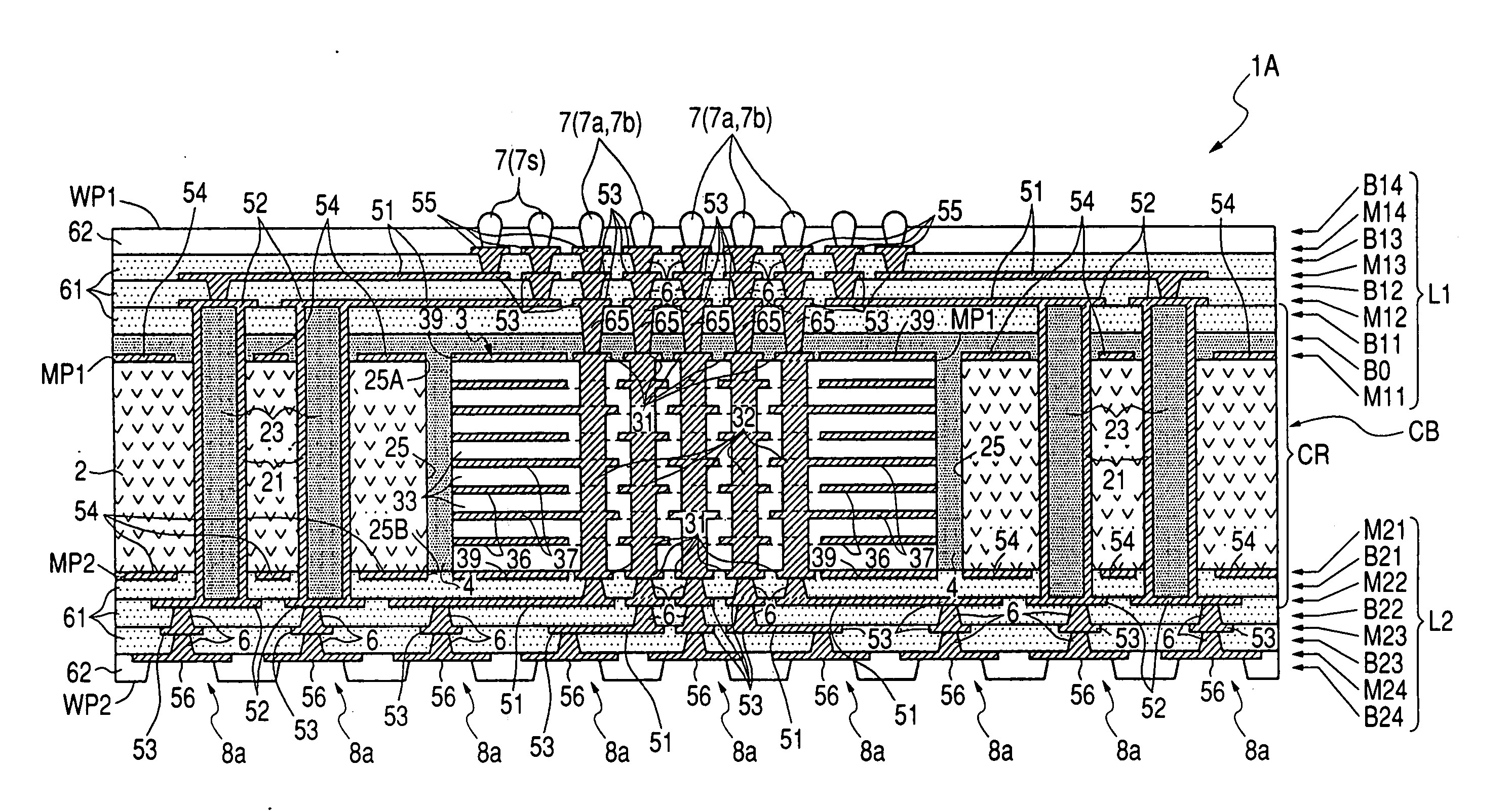
[0117] A wiring board according to a first embodiment of the present invention will be described below with reference to the drawings. FIG. 1 is a schematic sectional view showing the configuration of a wiring board 1A according to the first embodiment. In the following description, as for a plate-like member, a surface shown above in a figure will be called a first major surface WP1, MP1 and a surface shown below will be called a second major surface WP2, MP2. The wiring board 1A has a ceramic sub-core (laminated ceramic capacitor) 3 under solder bumps 7 in a core board CB. The use of the ceramic sub-core 3 shorten the lengths of interconnections between a semiconductor integrated circuit device (IC chip) C and the ceramic sub-core 3 contributes to reduction of the inductance components of the interconnections, which is important in reducing the switching noise of the IC chip C and stabilizing its operation power supply voltage. Since the ceramic sub-core 3 which is made of ceramic...

second embodiment

[0156] A wiring board according to a second embodiment of the invention will be described with reference to the drawings. FIG. 12 is a schematic sectional view showing the configuration of a wiring board 1B according to the second embodiment. The following description will mainly be directed to points that are different than in the wiring board 1A according to the first embodiment, and components having the same or corresponding components in the first embodiment will be given the same reference symbols as the latter and will not be described.

[0157] The wiring board 1B according to the second embodiment does not have the adjacent resin insulating layer B11 of the wiring board 1A according to the first embodiment. That is, in the first-major-surface-MP1-side wiring laminate L1, via conductors 6 penetrate through only a lowest resin insulating layer B10 and connect the conductor pads 31 (conductive layer M11) formed on the first major surface MP1 of the ceramic sub-core 3 to the cond...


PUM


Abstract

A wiring board comprising: a core board including a core body and a ceramic sub-core which is accommodated in a sub-core accommodation space that is a through-hole that communicates with major surfaces of the core body or a recess having an opening in a first major surface of the core body; and wiring laminates each formed by resin insulating layers and conductor layers laminated on each of major surfaces of the core board, wherein: a groove-filling portion which fills a gap between the core body and the ceramic sub-core is integral with a lowest resin insulating layer of the first-major-surface-side wiring laminate; and via conductors that are connected to respective conductor patterns formed on a first major surface of the ceramic sub-core penetrate through the lowest resin insulating layer.

Description

FIELD OF THE INVENTION [0001] The present invention relates to a wiring board having a core board that accommodates a ceramic sub-core mainly made of ceramics. BACKGROUND OF THE INVENTION [0002] Conventionally, to reduce the switching noise of a semiconductor integrate circuit device (hereinafter referred to as “IC chip”) and stabilize its operation power supply voltage, a capacitor is provided in a wiring board that is mounted with the IC chip. As for the manner of mounting the capacitor on the wiring board, as the lengths of interconnections between the IC chip and the capacitor increase, the inductance components of the interconnections increase and it becomes more difficult to attain the above effects sufficiently. It is therefore desirable that the capacitor be disposed as close to the IC chip as possible. JP-A-2005-39243 proposes a wiring board in which a core board located right under an IC chip accommodates a ceramic sub-core that incorporates a capacitor. SUMMARY OF THE INV...

Claims


Application Information

Patent Timeline
IPC IPC(8): H05K1/11H05K3/36
CPCH01L2224/13111Y10T29/49155H01L2224/81801H01L2224/97H01L2924/01005H01L2924/01013H01L2924/01027H01L2924/01029H01L2924/0103H01L2924/01033H01L2924/01046H01L2924/01047H01L2924/01051H01L2924/01059H01L2924/01075H01L2924/01078H01L2924/01079H01L2924/01082H01L2924/09701H01L2924/14H01L2924/15311H01L2924/19041H01L2924/30107H05K1/0231H05K1/112H05K1/142H05K1/162H05K1/185H05K3/4602H05K2201/096H05K2201/10674H05K2201/10712H01L2224/16Y10T29/49165Y10T29/49117Y10T29/4913H01L21/4857H01L21/568H01L21/6835H01L23/49822H01L23/50H01L24/81H01L24/97H01L2924/01006H01L2924/01019H01L2924/01024H01L2924/01041H01L2924/0105H01L2924/01055H01L2924/014H01L2224/16225H01L2224/16235Y10T29/49126Y10T29/49124Y10T29/49128H01L2224/81H01L2924/00011H01L2924/00014H01L2924/12042H01L2924/12044H01L2924/15787H01L2924/351H01L2924/00H01L2224/0401
Inventor MURAMATSU, MASAKIYURI, SHINJIORIGUCHI, MAKOTOURASHIMA, KAZUHIRO
Owner NGK SPARK PLUG CO LTD
Why Eureka
Try Eureka