Gradation display reference voltage generating circuit and liquid crystal driving device

US20060274005A1Active Publication Date: 2006-12-07SHENZHEN TOREY MICROELECTRONIC TECH CO LTD

Image

  • Gradation display reference voltage generating circuit and liquid crystal driving device
  • Gradation display reference voltage generating circuit and liquid crystal driving device
  • Gradation display reference voltage generating circuit and liquid crystal driving device

Examples


Embodiment Construction

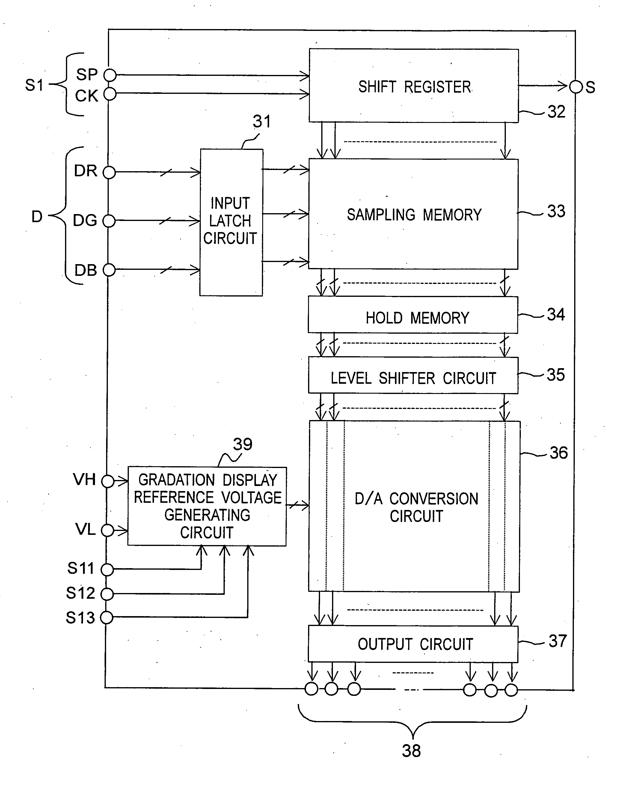
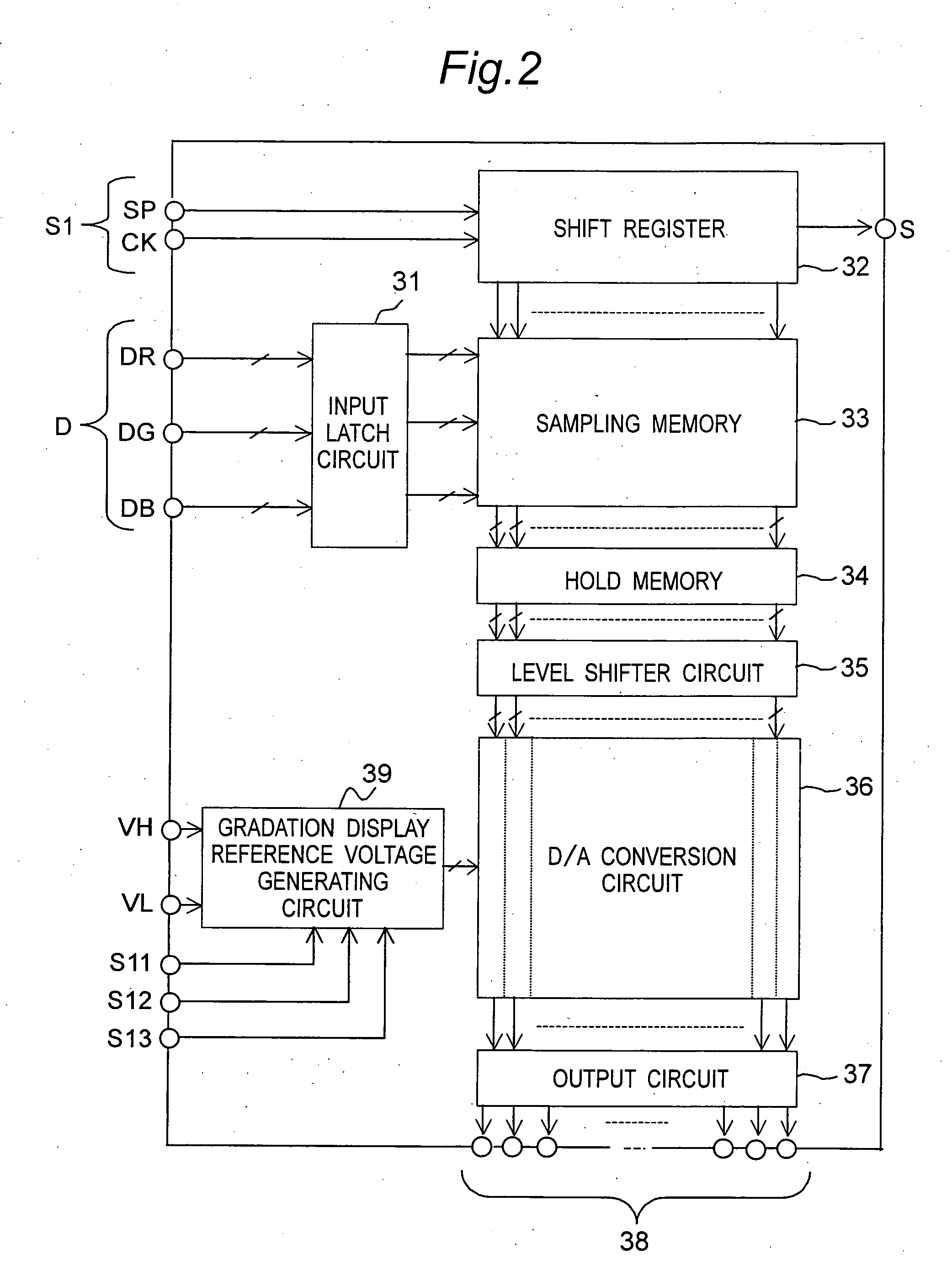
[0063] A gradation display reference voltage generating circuit and a liquid crystal driving device according to the present invention will be described in detail below based on the embodiments shown in the figures.

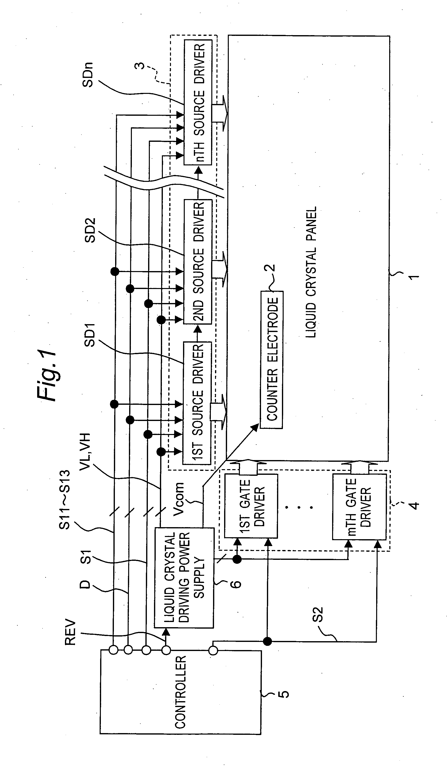
[0064]FIG. 1 is a block diagram showing the configuration of a liquid crystal display device having a liquid crystal driving device that employs a gradation display reference voltage generating circuit according to an embodiment of the present invention.

[0065] The liquid crystal display device has a TFT liquid crystal panel 1, a counter electrode 2 in the liquid crystal panel 1, a source driver section 3, a gate driver section 4, a controller 5, and a liquid crystal driving power supply 6. The source driver section 3, the gate driver section 4, the controller 5, and the liquid crystal driving power supply 6 constitute a liquid crystal driving device.

[0066] The controller 5 enters display data D and control signals S1 and S11 to S14 into the source driver section 3, whi...


PUM


Abstract

In a gradation display reference voltage generating circuit, first reference voltages (VH0 to VH63) produced by resistors for positive polarity (RH0 to RH64) of a first ladder circuit in a first reference voltage producing section (LDH) are output from reference voltage output terminals (T0 to T63), respectively, at the positive polarity drive, while second reference voltages (VL0 to VL63) produced by resistors for negative polarity (RL0 to RL64) of a second ladder circuit in a second reference voltage producing section (LDL) are output from the reference voltage outputs (T0 to T63), respectively, at the negative polarity drive. A resistance ratio of the resistors for positive polarity (RH0 to RH64) is different from a resistance ratio of the resistors for negative polarity (RL0 to RL64).

Description

CROSS-REFERENCE TO RELATED APPLICATIONS [0001] This nonprovisional application claims priority under 35 U.S.C. §119(a) on Patent Application No. 2005-166688 filed in Japan on Jun. 7, 2005, the entire contents of which are hereby incorporated by reference. BACKGROUND OF THE INVENTION [0002] The present invention relates to a gradation display reference voltage generating circuit and a liquid crystal driving device, and in particular to a gradation display reference voltage generating circuit used for a liquid crystal display device employing a line inversion method, and a liquid crystal driving device using it. [0003] Conventionally, there is a gradation display reference voltage generating circuit using intermediate voltages obtained by resistance division for driving the liquid crystal in an active matrix liquid crystal display device (see, for example, JP 11-272243 A). [0004] In the gradation display reference voltage generating circuit, the resistors used for resistance division ...

Claims


Application Information

Patent Timeline
07 Dec 2006
Publication
US20060274005A1
IPC
G09G3/36
CPC
G09G3/3614; G09G3/3688; G09G2320/0276; G09G2310/027; G09G3/3696; G09G3/20; G09G3/36
Inventors
MIYAZAKI, EISAKU