Arrangement of electronic semiconductor components on a carrier system for treating said semiconductor components with a liquid medium

a carrier system and electronic semiconductor technology, applied in electrical appliances, confectionery, sweetmeats, etc., can solve the problems of unfavorable liquid flow, increased cost, and special effort, and achieve the effect of preventing the damaging influence of liquid medium seeping into the gap, safe handling of semiconductor components, and avoiding the effect of liquid medium flowing into the gap

Inactive Publication Date: 2006-12-07
INFINEON TECH AG
View PDF12 Cites 8 Cited by
  • Summary
  • Abstract
  • Description
  • Claims
  • Application Information

AI Technical Summary

Benefits of technology

[0010] The invention is consequently based on the object of providing a detachable arrangement of electronic semiconductor components on a mechanically stable carrier system for safely handling the semiconductor components as products in the production process, in which the capillary action of the gap between the semiconductor components and the carrier system is reduced in a controlled manner and consequently the damaging influence of a liquid medium seeping into the gap is prevented.

Problems solved by technology

Alternatively, the capillary action of the gap may lead to undesired flowing of the liquid medium under the semiconductor component.
In the past, the damage to the semiconductor components has been minimized by frequent changing of the carrier system or by the thin wafers being handled for a short time, which however leads to a special effort being required and to increased costs, also on account of the susceptibility of the thin wafers to fracture.
However, the film material drastically limits the temperature range that is available for the further process, generally to below 100° C. A further major disadvantage of this method is that the requirement to remove the film again requires the thin wafer to be of a certain thickness, which must be great enough to withstand the mechanical forces during the detachment of the film.
However, future technologies require far smaller wafer and component thicknesses.

Method used


Image

  • Arrangement of electronic semiconductor components on a carrier system for treating said semiconductor components with a liquid medium
  • Arrangement of electronic semiconductor components on a carrier system for treating said semiconductor components with a liquid medium

Examples


Embodiment Construction

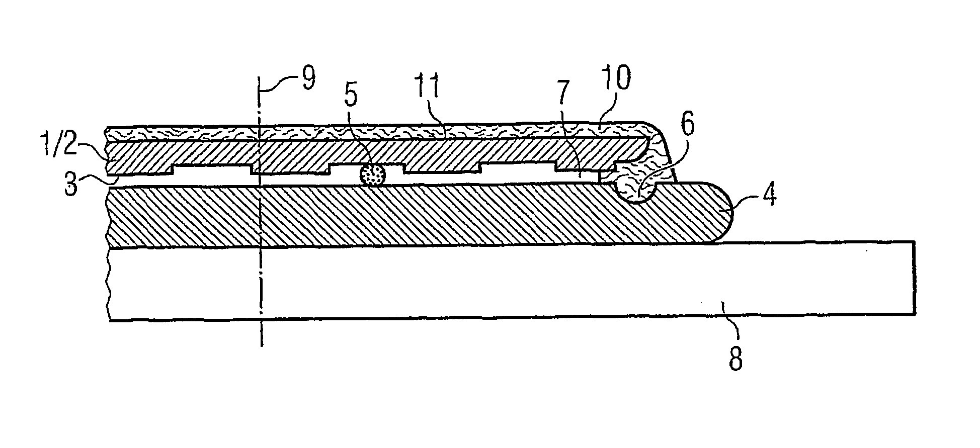
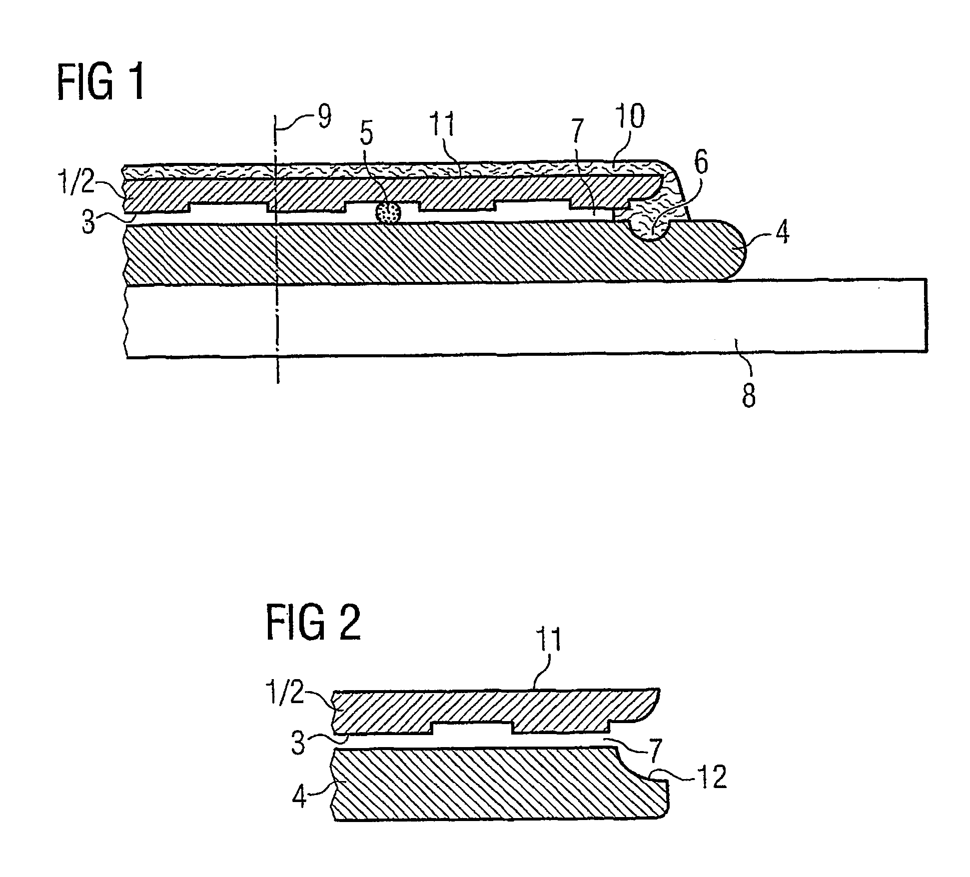
[0029] In the arrangement according to the invention of electronic semiconductor components 1 on a carrier system 4, as schematically represented in FIG. 1, the semiconductor components 1 in the wafer array are mounted with the active side 3, having a structure, downward (face down) on a round carrier system 4 by spot adhesion, so that balls of adhesive 5 detachably establish the connection between the semiconductor component 1, in this exemplary embodiment the wafer 2, and the carrier system 3 only at some locations.

[0030] The diameter of the carrier system 4 is greater than the diameter of the wafer 2. On the diameter that corresponds approximately to that of the wafer 2 the carrier system 4 has a channel 6 with a semicircular cross section, the depth of which in the exemplary embodiment represented corresponds approximately to the height of the gap 7 between the wafer 2 and the carrier system 4, so that the gap 7 is increased in the region of the channel 6 to twice the width.

[0...


PUM

PropertyMeasurementUnit
temperatureaaaaaaaaaa
thicknessaaaaaaaaaa
sizeaaaaaaaaaa

Abstract

The invention relates to an arrangement of electronic semiconductor components on a carrier system for treating the semiconductor components with a liquid medium. A semiconductor component is detachably mounted on the carrier system with the active side thereof in such a way that the arrangement comprises a gap at least in the edge region and partially between the semiconductor components and the carrier system. The aim of the invention is to provide a detachable arrangement of electronic semiconductor components on a mechanically stable carrier system for safely handling the semiconductor components during the production process, wherein the capillarity of the gap between the semiconductor components and the carrier system is reduced in a controlled manner, thus preventing the damaging effect of a liquid medium seeping into the gap. To this end, the surface of the carrier system is shaped in such a way that the gap is widened along the entire edge region thereof.

Description

[0001] This application is a continuation of co-pending International Application No. PCT / DE2004 / 002164, filed Sep. 29, 2004, which designated the United States and was not published in English, and which is based on German Application No. 203 18 462.9, filed Nov. 26, 2003, both of which applications are incorporated herein by reference.TECHNICAL FIELD [0002] The invention relates to an arrangement of electronic semiconductor components on a carrier system for treating the semiconductor components with a liquid medium. BACKGROUND [0003] The arrangement of an electronic semiconductor component with the active side downward (face down) on a carrier system, so that there is at least in certain portions an edge between the semiconductor component and the carrier system in a way corresponding to the topography of the semiconductor component, is very frequently encountered in semiconductor technology. A gap may be required for technical process-related reasons and the medium flowing aroun...

Claims


Application Information

Patent Timeline
Patent Type & Authority Applications(United States)
IPC IPC(8): A23G3/20H01L21/00H01L21/673H01L21/68
CPCH01L21/6704H01L21/6835H01L21/67075
Inventor BRADL, STEPHANMELZL, MICHAELSCHWAIGER, JOSEFSTACHE, THILO
Owner INFINEON TECH AG
Why Eureka
Try Eureka