Eureka AIR delivers breakthrough ideas for toughest innovation challenges, trusted by R&D personnel around the world.

Electrostatic protection device for semiconductor circuit

Active Publication Date: 2006-12-14
SK HYNIX INC
View PDF1 Cites 14 Cited by
  • Summary
  • Abstract
  • Description
  • Claims
  • Application Information

AI Technical Summary

Benefits of technology

[0009] Accordingly, the present invention has been made to solve the above-mentioned and other problems occurring in the prior art, and an object of the present invention is to provide an ESD protection device for a semiconductor circuit, which can prevent metal wires from being molten by the current concentration and drains from being attacked by the ESD.
[0010] It is another object of the present invention to provide an ESD protection device for a semiconductor circuit, which can achieve a uniform ESD through the entire ESD protection device.

Problems solved by technology

A semiconductor integrated circuit (IC) could be damaged when it comes in contact with a charged human body or machine.
An unhealthy dose of static electricity or electrostatic discharge (ESD) charges from a human body or a machine could be discharged into the semiconductor IC through its contacting external pin(s) and pad(s), such that an excessive current of large energy introduced into the semiconductor IC may cause the internal damage.
Therefore, when excessive current flowing due to ESD charges is concentrated at the end of each common drain 4 connected to the pad 1, the metal wires M1˜M7 at the connected end may melt or the connected end of each drain 4 itself may be damaged by the ESD.
Further, the conventional structure as shown in FIG. 1 could be problematic when the excessive current passes through the pickup 5 surrounding the multi-fingered transistor structure.
As a result, the entire NMOS “finger” transistors of the conventional ESD protection device may yield non-uniform results at the time of bipolar turn-on.

Method used


Image

  • Electrostatic protection device for semiconductor circuit
  • Electrostatic protection device for semiconductor circuit
  • Electrostatic protection device for semiconductor circuit

Examples


Embodiment Construction

[0023] Hereinafter, several preferred embodiments of the present invention will be described with reference to the accompanying drawings.

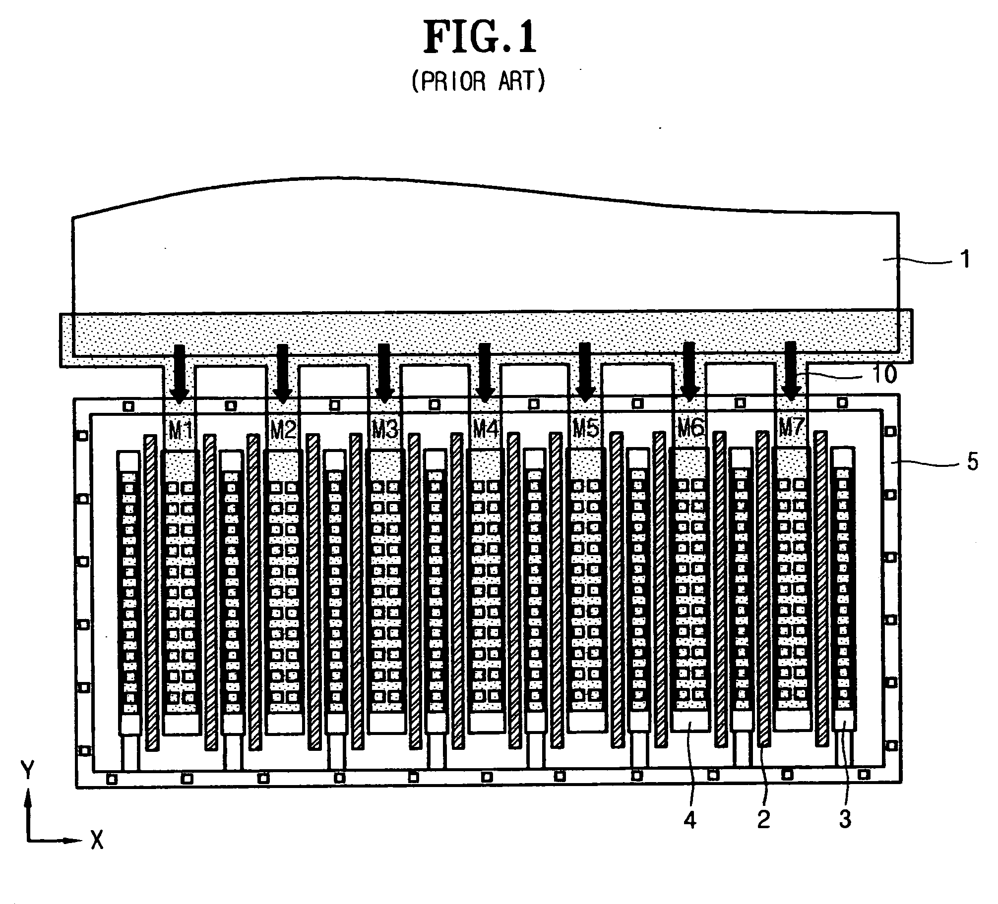
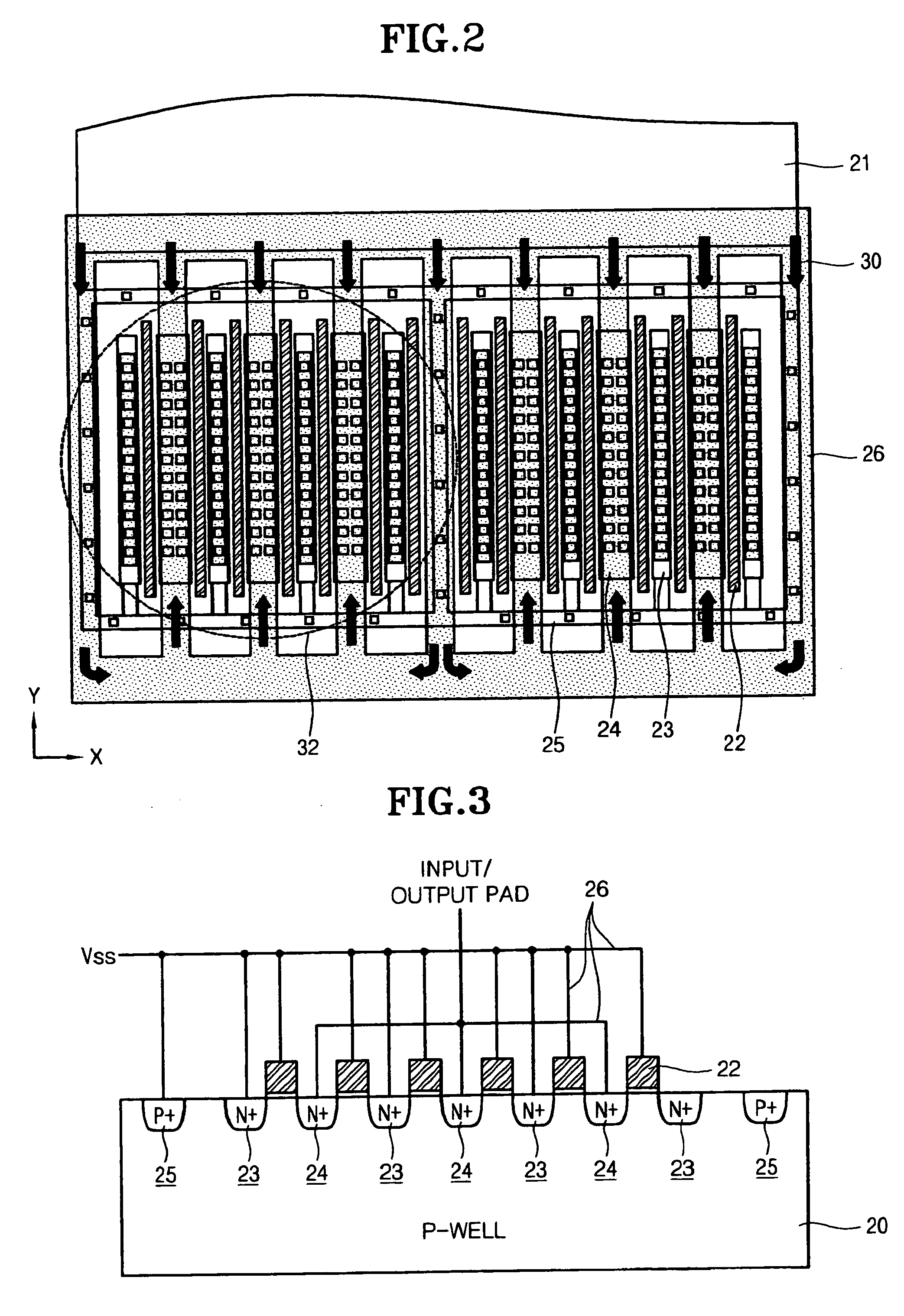
[0024]FIG. 2 shows the multi-fingered transistor layout of an ESD protection device for a semiconductor circuit according to an embodiment of the present invention.

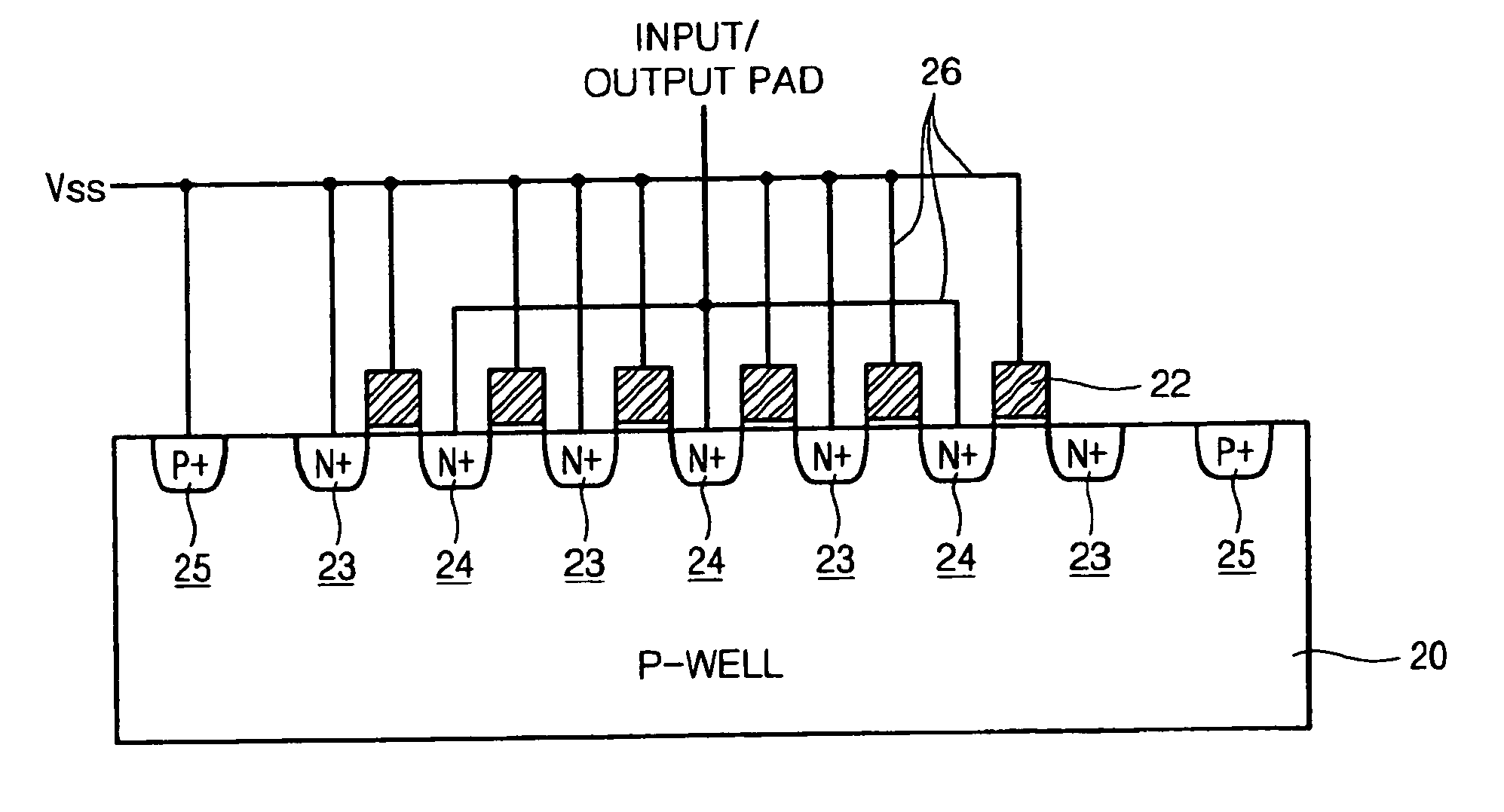
[0025] As shown, an ESD protection device for a semiconductor circuit according to an embodiment of the present invention includes at least two sets of transistor fingers 32 spaced apart, for example, in the X direction, and a well pickup 25 extending around the entire each set of transistor fingers 32. In this embodiment, the finger transistor is an NMOS transistor although it should be apparent that use of other comparable transistors is also within the scope of the present invention. Each NMOS finger transistor in the set of transistors 32 has a gate 22, a source 23, and a drain 24, which is also connected to the gate of the adjacent transistor. The finger transistors in each set 32...


PUM


Abstract

The electrostatic protection device includes a semiconductor substrate having a well formed therein. At least two sets of transistor fingers, for example the NMOS type, are spaced apart from each other. Each set of the MOS fingers includes multiple gates arranged in parallel to each other in one direction, and sources and drains alternately arranged at both sides of the gates in the semiconductor substrate. A well pickup surrounding every set of the transistor fingers and extending between any two set of the fingers is formed. Metal wires are connected to at least two portions of each of the drains and are also connected to an input / output pad to which Electrostatic Discharge (ESD) excessive current is introduced.

Description

BACKGROUND OF THE INVENTION [0001] 1. Field of the invention [0002] The present invention relates generally to an electrostatic protection device for a semiconductor circuit, and more particularly to a connection structure of an electrostatic protection device for preventing damage due to discharge of electrostatic charges. [0003] 2. Description of the Prior Art [0004] A semiconductor integrated circuit (IC) could be damaged when it comes in contact with a charged human body or machine. An unhealthy dose of static electricity or electrostatic discharge (ESD) charges from a human body or a machine could be discharged into the semiconductor IC through its contacting external pin(s) and pad(s), such that an excessive current of large energy introduced into the semiconductor IC may cause the internal damage. [0005] Therefore, an ESD protection device is typically formed in a semiconductor IC between a pad and its internal circuit in order to protect the important circuits from such elec...

Claims


Application Information

Patent Timeline
IPC IPC(8): H01L29/76
CPCH01L27/0266H01L29/78H01L29/41758H01L27/04
Inventor LEE, YOON SUNGKWAK, KOOK WHEE
Owner SK HYNIX INC
Why Eureka
Eureka Blog
Learn More