Laminated semiconductor package

a semiconductor chip and laminate technology, applied in semiconductor devices, semiconductor/solid-state device details, electrical devices, etc., can solve the problems of reducing the reliability of system operation, difficult to support a larger number of pins in a semiconductor chip, and a large heating value of a semiconductor chip including a logic device, etc., to achieve the effect of suppressing the reduction of operation reliability

Active Publication Date: 2006-12-14
SHINKO ELECTRIC IND CO LTD
View PDF12 Cites 13 Cited by
  • Summary
  • Abstract
  • Description
  • Claims
  • Application Information

AI Technical Summary

Benefits of technology

[0042] According to the invention, it is possible to provide a laminated semiconductor package including a plurality of semiconductor chips, that suppresses reduction in the reliability of operation caused by the influence of thermal radiation from a semiconductor chip and supports a semiconductor chip having multiple pins.

Problems solved by technology

A semiconductor chip including a logic device generally has a problem of a large heating value.
This degrades the reliability of system operation.
One of the problems with the laminated package 400 is that it is difficult to support a larger number of pins in a semiconductor chip mounted on the package 200.
This makes it difficult to form a connecting section for connecting the upper and lower packages, on a surface area where the semiconductor chip is mounted.
In recent years, even a memory semiconductor chip has accommodated more and more pins so that the structure of the package 400 could not support the semiconductor chip having multiple pins.
It is also difficult for this type of laminated package to mount a semiconductor chip having multiple pins and including a logic device, on the upper layer.

Method used


Image

  • Laminated semiconductor package
  • Laminated semiconductor package
  • Laminated semiconductor package

Examples


first embodiment

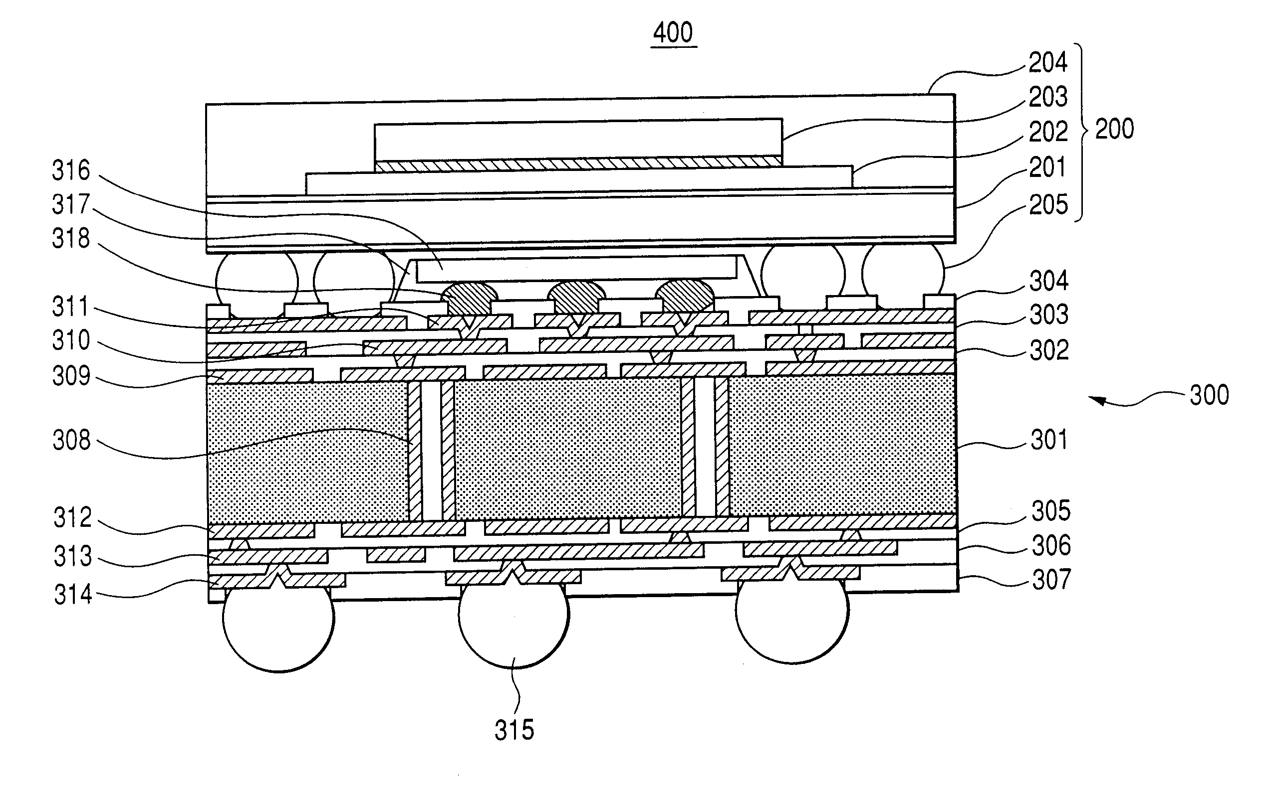
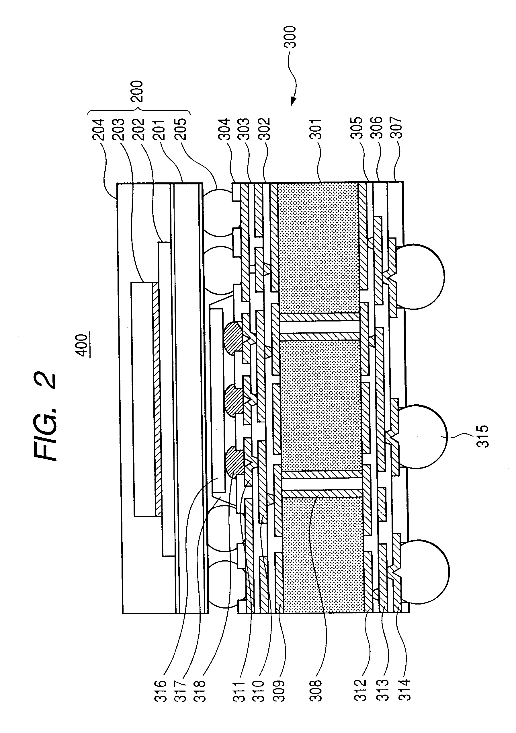
[0048]FIG. 3 schematically shows a laminated semiconductor package 500 according to a first embodiment of the invention.

[0049] Referring to FIG. 3, the laminated semiconductor package 500 has an exemplary structure where a package 600 configured with an F-BGA is laminated on a package 700 configured with a substrate incorporating a semiconductor chip.

[0050] The package 700 has a structure where an insulating layer 701 made of a resin material such as epoxy with a semiconductor chip 715 embedded therein. Further, the insulating layer 701 has a wiring structure including via-plugs 703, 705, 707, 709 and pattern wirings 704, 706, 708, 710.

[0051] Among the pattern wirings, a solder resist layer 711 having an opening is formed on the pattern wiring 710 as the top layer (the face side where the package 600 is laminated). A connection layer 712 for connection to the package 600 is formed on the pattern wiring 710 exposed from the opening. The connection layer 712 is for example an Au / Ni...


PUM


Abstract

A laminated semiconductor package includes: a first package having: an insulating layer; a first semiconductor chip embedded in the insulating layer; a wiring connected to the first semiconductor chip; a first connecting section which is formed on a first face side of the insulating layer and connected to the wiring; and a second connecting section which is formed on a second face side of the insulating layer and connected to the wiring, the second face side being opposite to the first face side; and a second package having: a second semiconductor chip; and a third connecting section connected to the second semiconductor chip. In the laminated semiconductor chip, the first package and the second package are laminated one on the other, and the second connecting section and the third connecting section are connected to each other.

Description

[0001] This application claims foreign priority based on Japanese Patent application No. 2005-171855, filed Jun. 13, 2005, the content of which is incorporated herein by reference in its entirety. BACKGROUND OF THE INVENTION [0002] 1. Field of the Invention [0003] The present invention relates to a semiconductor package, and in particular to a laminated semiconductor package in which semiconductor chip packages are laminated. [0004] 2. Description of the Related Art [0005] In recent years, there have been proposed a variety of SiPs (System-in Packages) where a plurality of semiconductor chips is mounted on a single package in order to provide a predetermined system by the single package. [0006] For example, FIG. 1 schematically shows a structure of a 3-chip-stack F-BGA (ball grid array) as one of the forms of SiP. [0007] Referring to FIG. 1, a package 100 shown in FIG. 1 has a structure where an interposer 101 made of organic material, for example, with semiconductor chips 102, 103,...

Claims


Application Information

Patent Timeline
Patent Type & Authority Applications(United States)
IPC IPC(8): H01L23/02
CPCH01L23/5389H01L25/105H01L2225/1035H01L2924/3511H01L2224/32225H01L2224/16225H01L2225/1058H01L2225/1023H01L2924/15331H01L2924/15311H01L2224/73204H01L2225/06562H01L2924/12044H01L2924/00012H01L2924/00H01L2924/00011H01L2924/00014H01L2224/0401H01L23/12
Inventor YAMANO, TAKAHARU
Owner SHINKO ELECTRIC IND CO LTD
Why Eureka
Try Eureka