Thin film transistor substrate and display device including the same

A thin-film transistor and substrate technology, which is applied in the direction of transistors, semiconductor devices, and electric solid-state devices, can solve the problems of thin-film transistor drive stability and reliability reduction, damage, etc., achieve excellent reliability and drive stability, and suppress insulation glitch effect

Pending Publication Date: 2022-07-01
LG DISPLAY CO LTD
View PDF0 Cites 0 Cited by
  • Summary
  • Abstract
  • Description
  • Claims
  • Application Information

AI Technical Summary

Problems solved by technology

[0009] However, the oxide semiconductor layer of the oxide semiconductor thin film transistor is damaged during a patterning process including etching or annealing of the manufacturing process, so that the driving stability and reliability of the thin film transistor may decrease

Method used


Image

  • Thin film transistor substrate and display device including the same
  • Thin film transistor substrate and display device including the same
  • Thin film transistor substrate and display device including the same

Examples


Embodiment Construction

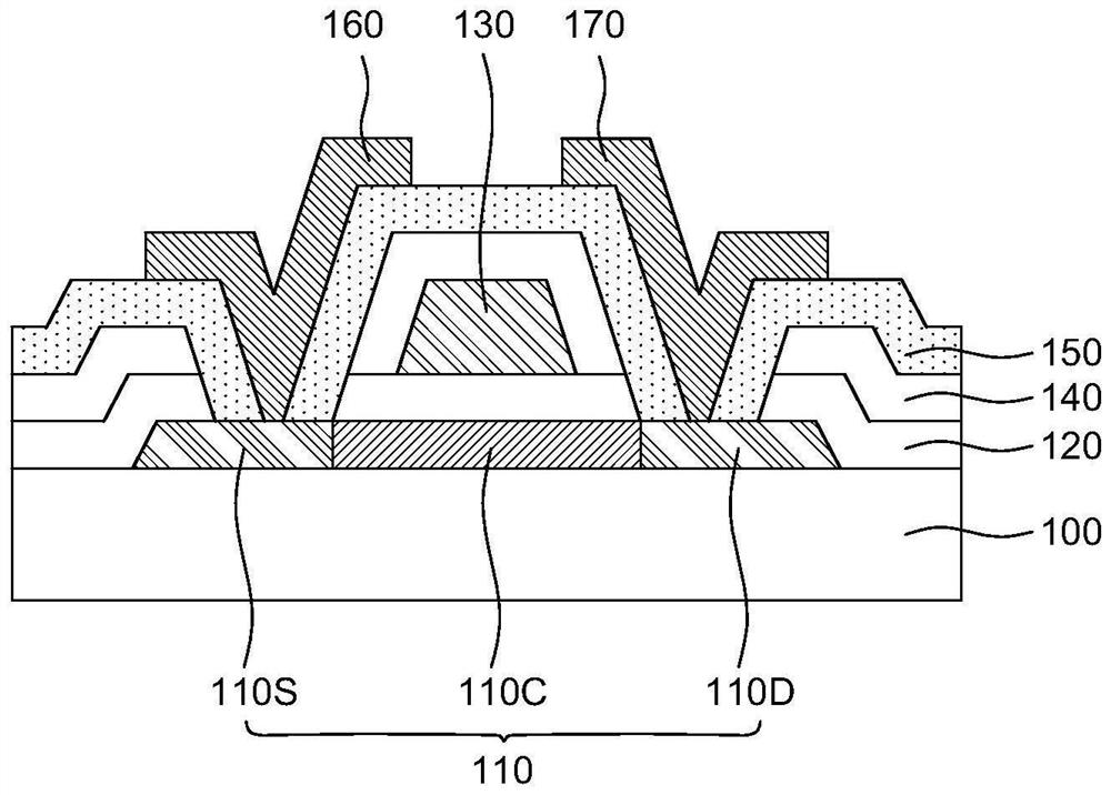
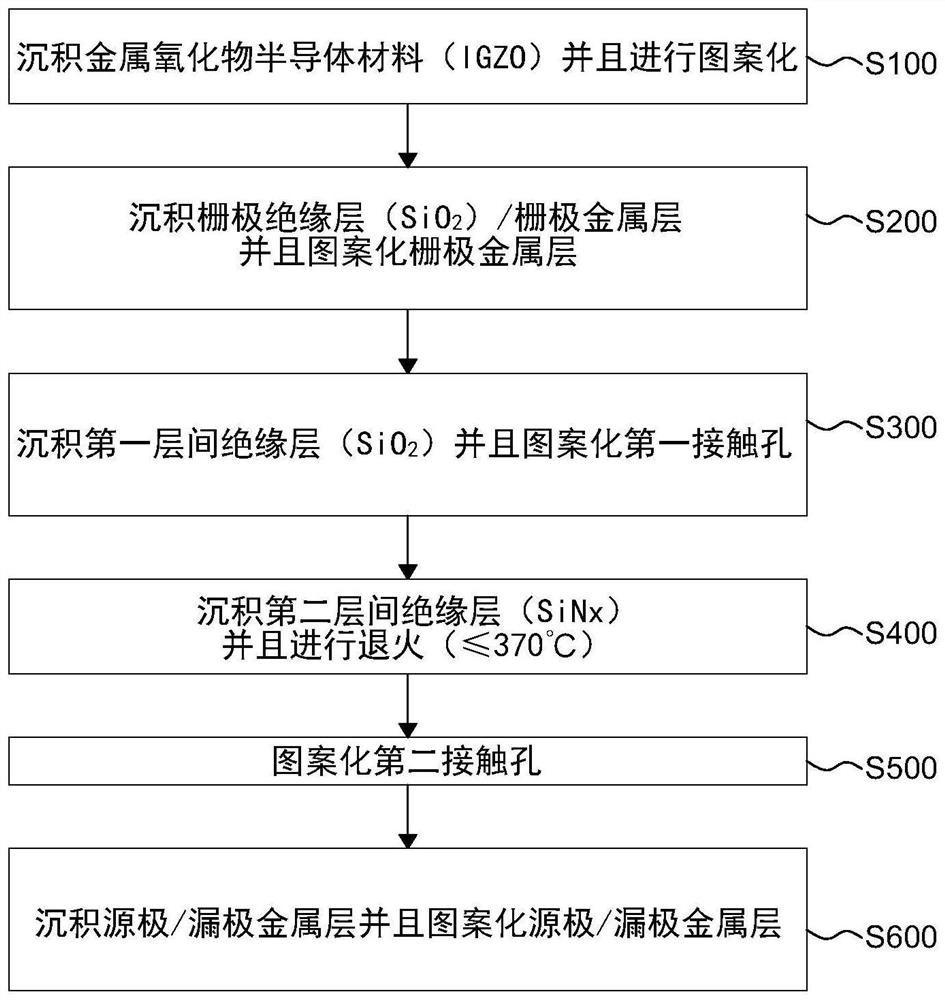
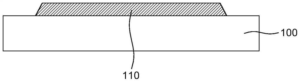
[0034] Advantages and features of the present disclosure, and methods for achieving them, will become apparent by reference to the exemplary embodiments described in detail below and the accompanying drawings. However, the present disclosure is not limited to the exemplary embodiments disclosed herein, but will be implemented in various forms. The exemplary embodiments introduced herein are provided so that this disclosure will be thorough and complete, and will fully convey the spirit of the present disclosure to those skilled in the art. The present disclosure is limited only by the scope of the claims.

[0035] The shapes, sizes, ratios, angles, numbers, etc. shown in the drawings for describing exemplary embodiments of the present disclosure are merely examples, and the present disclosure is not limited thereto. Throughout the specification, like reference numerals refer to like parts. Also, in the following description, a detailed explanation of known related art may be...


PUM


Abstract

The present disclosure relates to a thin film transistor substrate and a display device including the same. An exemplary embodiment of the present disclosure provides a thin film transistor including an oxide semiconductor layer on a substrate; a gate insulating layer on the oxide semiconductor layer; a gate electrode on the gate insulating layer at least partially overlapping the oxide semiconductor layer; an interlayer insulating layer on the gate electrode; and a source electrode and a drain electrode on the interlayer insulating layer. The oxide semiconductor layer includes a channel portion overlapping the gate electrode and a connection portion at least partially not overlapping the gate electrode, the source electrode and the drain electrode are in contact with the connection portion of the oxide semiconductor layer, the interlayer insulating layer is in contact with the connection portion of the oxide semiconductor layer, a hydrogen concentration of the connection portion is higher than a hydrogen concentration of the channel portion, and a hydrogen concentration of the interlayer insulating layer is lower than a hydrogen concentration of the channel portion. And the interlayer insulating layer, the source electrode, and the drain electrode are in contact with the connection portion.

Description

[0001] CROSS-REFERENCE TO RELATED APPLICATIONS [0002] This application claims priority to Korean Patent Application No. 10-2020-0188805 filed in the Korean Intellectual Property Office on December 31, 2020, the disclosure of which is incorporated herein by reference. technical field [0003] The present disclosure relates to a thin film transistor substrate and a display device including the thin film transistor substrate. Background technique [0004] Thin film transistors can be fabricated on glass substrates or plastic substrates, so that they are widely used as switching elements or driving elements of display devices such as liquid crystal display devices or organic light emitting devices. [0005] According to the material constituting the active layer, thin film transistors can be classified into amorphous silicon thin film transistors, polysilicon thin film transistors, and oxide semiconductor thin film transistors. An amorphous silicon thin film transistor uses a...

Claims


Application Information

Patent Timeline
Patent Type & Authority Applications(China)
IPC IPC(8): H01L29/786H01L29/417H01L21/34
CPCH01L29/7869H01L29/41733H01L21/34H01L29/66969H01L27/1225H01L27/1248H01L27/124H01L29/4908H01L27/1259H01L27/1237
Inventor 徐诚模
Owner LG DISPLAY CO LTD
Why Eureka
Try Eureka