Unlock instant, AI-driven research and patent intelligence for your innovation.
Semiconductor device, stacked semiconductor device, and manufacturing method for semiconductor device
Active Publication Date: 2006-12-14
III HLDG 12 LLC
View PDF21 Cites 48 Cited by
Summary
Abstract
Description
Claims
Application Information
AI Technical Summary
This helps you quickly interpret patents by identifying the three key elements:
Problems solved by technology
Method used
Benefits of technology
Benefits of technology
[0013] Further, it is another object of the present invention to reduce, through a simple process, damage to a semiconductor chip or the like in such a configuration that an external connection terminal is exposed from a resin layer.
[0015] In the configuration, the first external connection terminal has the exposed surface which is exposed from the surface of the resin layer, and the exposed surface of the first external connection terminal and the surface of the resin layer form a single plane. Therefore, at a time of stacking another semiconductor device on the semiconductor device of the present invention, the first external connection terminal is connected with an external connection terminal of the upper semiconductor device, even if the external connection terminal of the upper semiconductor device is low. Incidentally, in a case where external connection terminals of the upper semiconductor device are arranged at a narrow pitch, the height of each of the external connection terminals is low. However, with the configuration, the resin layer does not block the external connection terminal from reaching the first external connection terminal. Thus, it is not necessary to lower the resin layer for the purpose of acquiring a connection between the external connection terminals. As a result, the semiconductor device of the present invention is high in its connection reliability, and is easily manufactured without a need for a technology to reduce the thickness of the semiconductor device, such a technology being a technology for reducing the thickness of the semiconductor chip, a technology for lowering the loop of the wire, or the like.
[0016] Further, instead of exposing the wiring layer formed on the semiconductor chip, the above described first external connection terminal is used for acquiring the connection with the upper semiconductor device. This reduces damage to the semiconductor chip even if the semiconductor device is sealed with a resin by using a transfer mold or the like.
[0018] With the configuration, it is possible to manufacture a semiconductor device in which (i) a first external connection terminal having the exposed surface which is exposed from a surface of the resin layer, and (ii) the exposed surface and the surface of the resin layer form a single plane. Thus, at a time of stacking another semiconductor device on the semiconductor device, the semiconductor devices are connected with each other, even if an external connection terminal of the upper semiconductor device is low. Incidentally, in a case where external connection terminals of the upper semiconductor device are arranged at a narrow pitch, the height of each of the external connection terminals is low. However, with the configuration, the resin layer does not block the external connection terminal from reaching the first external connection terminal. Thus, with the manufacturing method of the present invention for the semiconductor device, it is not necessary to lower the resin layer for the purpose of acquiring a connection with the upper semiconductor device. As a result, the method of the present invention allows easy manufacturing of a semiconductor device which is high in its connection reliability, and the method does not require a technology to reduce the thickness of the semiconductor device, such a technology being a technology for reducing the thickness of the semiconductor chip, a technology for lowering the loop of the wire, or the like.
[0021] In the configuration, the sub step of sealing is carried out after the external connection terminal is deformed by pressing the mold against the external connection terminal. With this simple process, it is possible to expose, from the resin layer, the exposed surface of the external connection terminal, and to form a single plane including the exposed surface and the surface of the resin layer. Thus, a semiconductor device is easily manufactured.
Problems solved by technology
This causes technical difficulty in the production of the semiconductor device 100.
A similar problem occurs in a case of stacking semiconductor devices illustrated in FIG. 16.
As a result, a strong stress is applied to the semiconductor chip 103, and this strong stress may cause damage to the semiconductor chip 103.
Method used
Image
Click on the blue label to locate the original text in one second.
Reading with bidirectional positioning of images and text.
Examples
example 1
ALTERNATIVE EXAMPLE 1
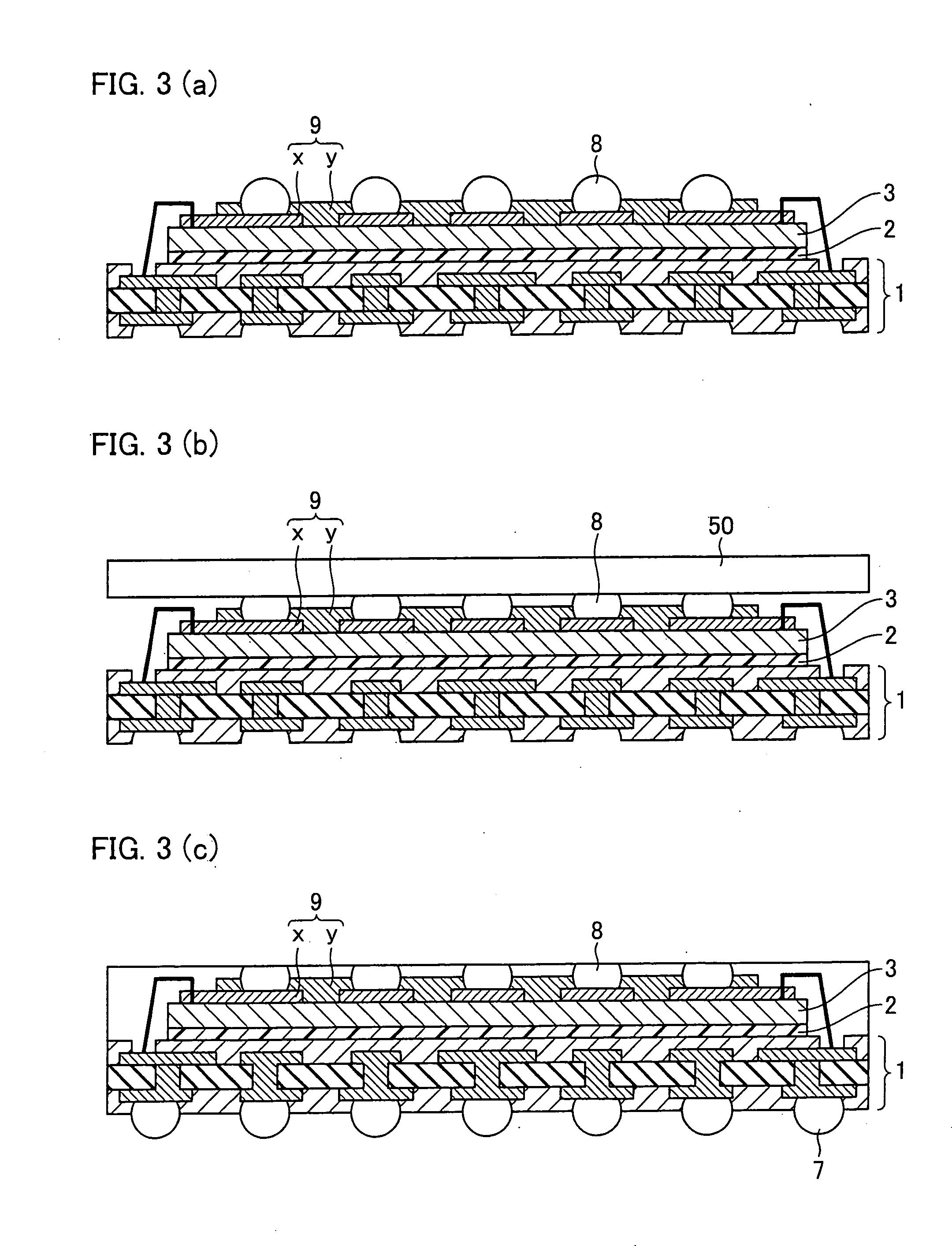
[0061]FIG. 4 is a cross sectional view illustrating a configuration of a semiconductor device 20a of Alternative Example 1. As illustrated in FIG. 4, a semiconductor chip 3 in the semiconductor device 20a is connected to a base substrate 1 by a flip-chip bonding using a bump 10, instead of connecting the semiconductor chip 3 and the base substrate 1 via a wire 4.
[0062] The semiconductor device 20a has the same configuration as that of the foregoing semiconductor device 20, except for the above described point.
[0063] As described, the flip-chip bonding technique is used in the semiconductor device 20a of the present alternative example, so that the semiconductor chip 3 is mounted on the base substrate 1 at a higher density.
[0064] A method for manufacturing this semiconductor device 20a is the same as the foregoing manufacturing method for the semiconductor device 20, except in that a flip-chip bonding is carried out for connecting the semiconductor chip 3 with...
example 2
ALTERNATIVE EXAMPLE 2
[0065]FIG. 5 is a cross sectional view illustrating a configuration of a semiconductor device 20b of Alternative Example 2. In the foregoing semiconductor devices 20 and 20a, the wiring layer 9 is directly formed on the semiconductor chip 3. However, in the semiconductor device 20b, a wiring layer 9 is formed on a supporting member 11. This wiring layer 9 on the supporting member 11 is mounted on an adhesive layer 12 which is provided on a semiconductor chip 3. As described, the wiring layer 9 is formed on the supporting member 11, and the wiring layer 9 on the supporting member 11 is mounted on the adhesive layer 12 on the semiconductor chip 3. With this configuration, a stress applied to the semiconductor chip 3 is reduced by the supporting member 11 and the adhesive layer 12. Thus, damage to the semiconductor chip 3 is reduced. The supporting member 11 and the adhesive layer 12 are insulative members. By adopting, for these members, a material whose elasticit...
example 3
ALTERNATIVE EXAMPLE 3
[0070]FIG. 6 is a cross sectional view illustrating a configuration of a semiconductor device 20c of Alternative Example 3. The configuration of the semiconductor device 20c is substantially the same as the semiconductor device 20b of Alternative Example 2. However, as illustrated in FIG. 6, the configuration of the semiconductor device 20c differs from the semiconductor device 20b in that a spacer layer 13 is provided on an adhesive layer 18 which is provided on a semiconductor chip 3.
[0071] With the provision of the spacer layer 13, a sufficient space for a wire 4 is acquired between the semiconductor chip 3 and an adhesive layer 12. Accordingly, in the semiconductor device 20c of the present alternative example, the wire 4 is not extended through the adhesive layer 12. This improves the reliability of the connection between the semiconductor chip 3 and the wire 4. Further, the supporting member 11 and the spacer layer 13 can be made of a heat conductive mate...
PUM
Abstract
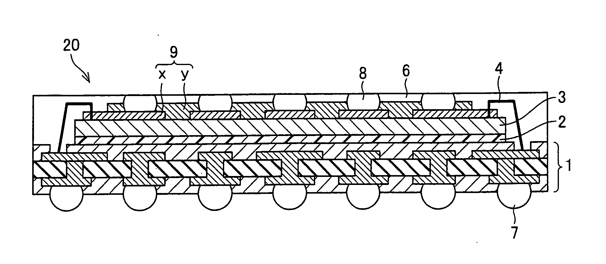
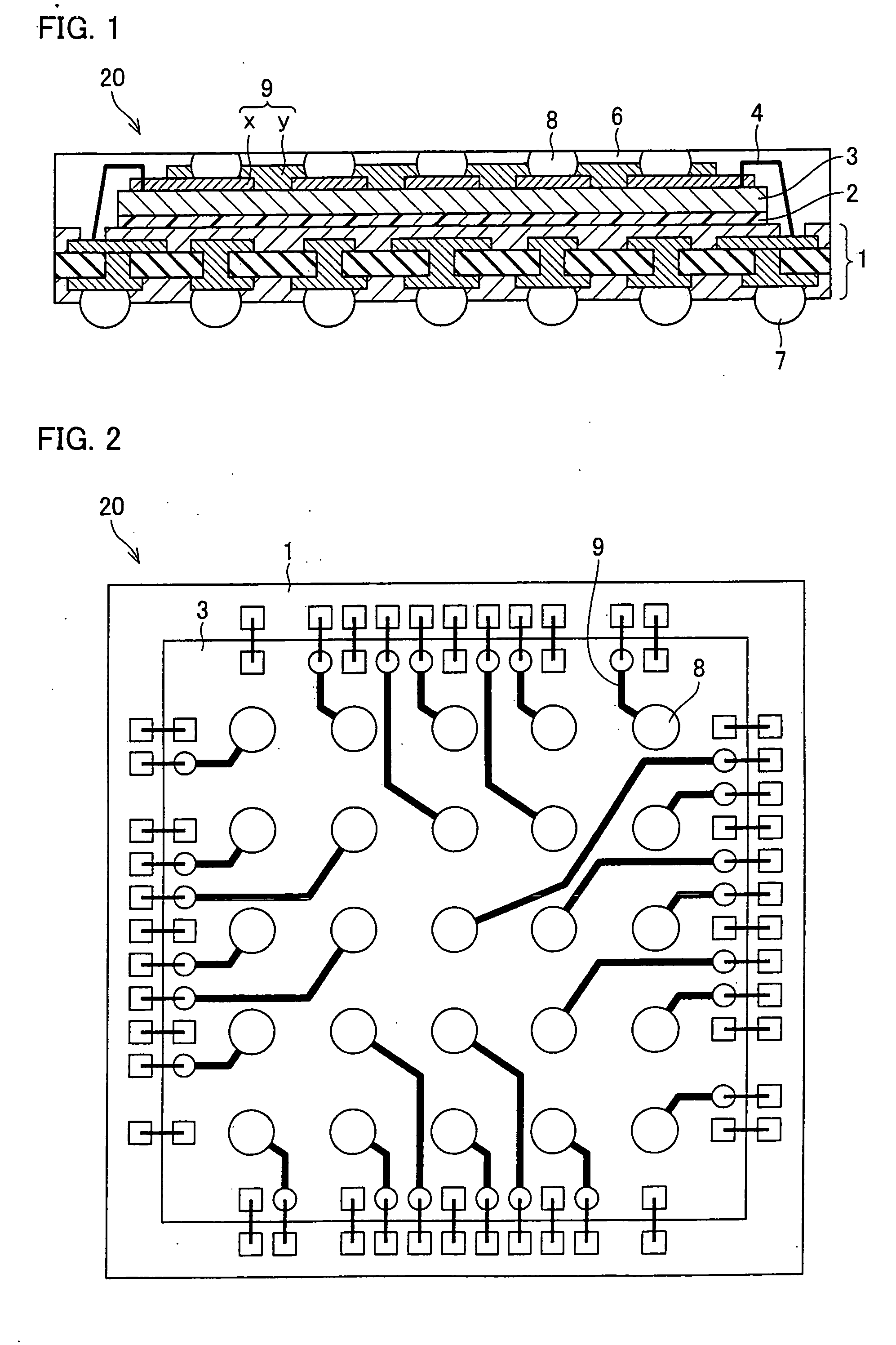
A semiconductor device includes: a base substrate; a semiconductorchip formed on the base substrate in such a manner that an adhesive layer is interposed between the semiconductorchip and the base substrate; a resin layer covering at least a portion of the semiconductor chip; and an external connection terminal electrically connected to the base substrate via a wiring layer. The external connection terminal is in the same plane as the surface of the resin layer, and is exposed from the resin layer. With this configuration, it is possible to provide a semiconductor device of a lower stage, and a stacked semiconductor device, each of which is high in connection reliability in a case of stacking plural semiconductor devices, no matter if a connection terminal of a semiconductor device stacked on an upper stage is low.
Description
[0001] This Nonprovisional application claims priority under 35 U.S.C. § 119(a) on Patent Application No. 171730 / 2005 filed in Japan on Jun. 10, 2005, the entire contents of which are hereby incorporated by reference. FIELD OF THE INVENTION [0002] The present invention relates to: (i) a semiconductor device having thereon a semiconductor chip; (ii) a stacked semiconductor device in which a plurality of semiconductor devices are stacked; and (iii) a manufacturing method for a semiconductor device. BACKGROUND OF THE INVENTION [0003] Smaller and lighter electronic devices having more advanced functions have been developed. Under such circumstances, it is required that semiconductor devices be more densely packaged. In response to such a requirement, for example, Japanese Unexamined Patent Publications No. 135267 / 1998 (Tokukaihei 10-135267; published on May 22, 1998) and No. 172157 / 2004 (Tokukai 2004-172157; Published on Jun. 17, 2004) suggest a method which allows higher density packag...
Claims
Application Information
Patent Timeline
Application Date:The date an application was filed.
Publication Date:The date a patent or application was officially published.
First Publication Date:The earliest publication date of a patent with the same application number.
Issue Date:Publication date of the patent grant document.
PCT Entry Date:The Entry date of PCT National Phase.
Estimated Expiry Date:The statutory expiry date of a patent right according to the Patent Law, and it is the longest term of protection that the patent right can achieve without the termination of the patent right due to other reasons(Term extension factor has been taken into account ).
Invalid Date:Actual expiry date is based on effective date or publication date of legal transaction data of invalid patent.

