
Image displaying apparatus

Inactive Publication Date: 2006-12-14
HARUNA FUMIO +1
View PDF0 Cites 93 Cited by
  • Summary
  • Abstract
  • Description
  • Claims
  • Application Information

AI Technical Summary

Benefits of technology

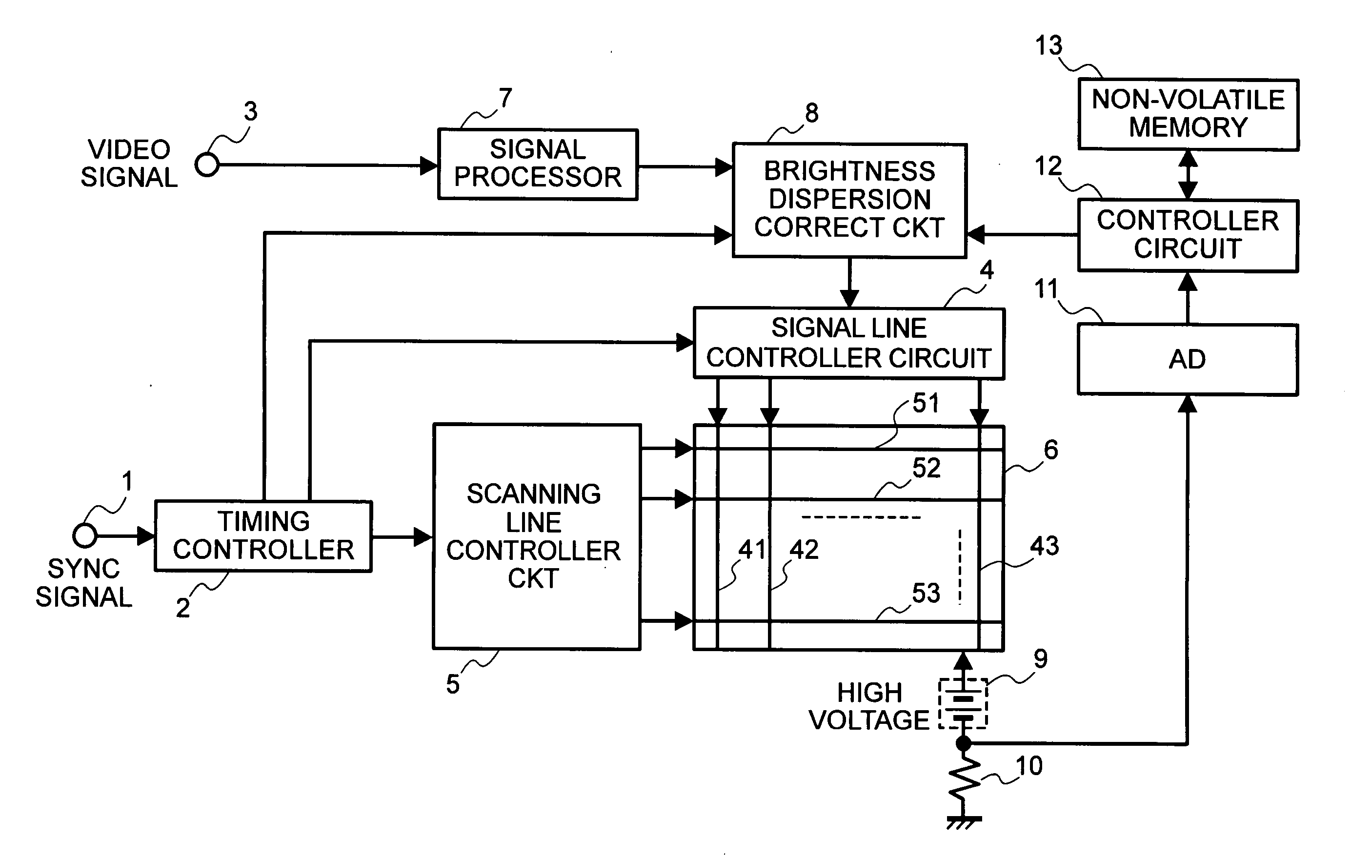
[0008] An object according to the present invention, therefore, is to provide a technology for enabling to display a picture of high quality, reducing the unevenness in brightness, through correcting the unevenness in brightness of the electron sources.
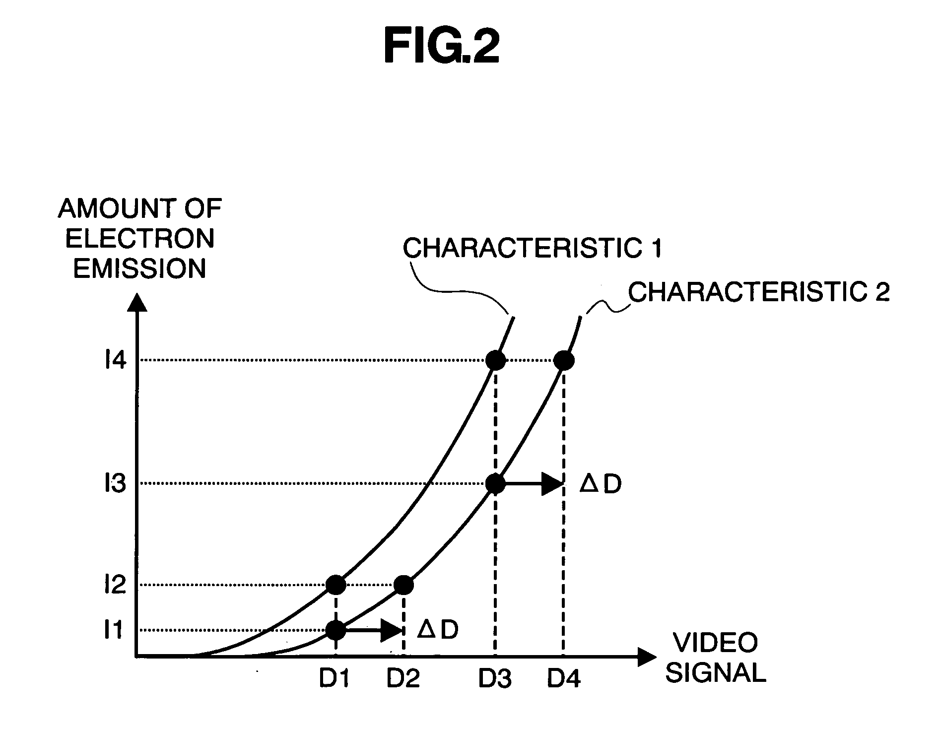
[0011] With such the structures as was mentioned above, the video signal corresponding to the electron source, which is determined to be the correction point, is corrected by the first correction value memorized, while the video signal(s) other than that is / are corrected by the second correction value, which is obtained from the memorized correction value through calculation thereof. Accordingly, with the structures according to the present invention, it is sufficient to determine the correction values, not for all the electron sources, but only corresponding to the number of pieces of the correction points; therefore, the time for measuring an amount of electron emission for obtaining the correction value can be reduced. Also, since there is no need of memorizing the correction values to correct the unevenness or dispersion of each the electron source, for the entire electron sources, therefore a capacity can be reduced for a memory.
[0012] According to the present invention, it is possible to correct the dispersion in brightness of the electron sources, preferably, and thereby enabling to obtain a display of high quality with reducing the unevenness in the brightness thereof.

Problems solved by technology

However, the anode current for one (1) pixel (i.e., one (1) piece of electron source) is actually very small (in a degree of about 1 μA), and for this reason, an error comes to be large in the detection thereof.
Also, when detecting the anode current for each one (1) pixel, a large amount of time is necessary.
Also, the correction values must be memorized corresponding to all of the electron sources, and therefore a large amount of memory capacity is necessary, too.

Method used


Image

  • Image displaying apparatus
  • Image displaying apparatus
  • Image displaying apparatus

Examples


embodiment 2

[0059] Next, explanation will be given about a second embodiment of the FED-type image displaying apparatus, according to the present invention. FIG. 10 is a block diagram for showing the interpolation circuit 85, for showing the second embodiment according to the present invention, and within the interpolation circuit 85 shown in this FIG. 10, the elements attached with the reference numerals, being same to those shown in FIGS. 5 and 7 according to the first embodiment, have the same functions thereof. An aspect of the second embodiment differing from the first embodiment shown in FIGS. 5 and 7 lies in that there are provided a plural number of the memories for use of correction data, corresponding to a plural number of predetermined gradations, and accompanying this, there are also provided a plural number of the interpolation circuits. With this, the correction data can be changed depending on the gradation of the video signal, and thereby correcting the brightness dispersion wit...


PUM


Abstract

An image displaying apparatus, comprises: a plural number of electron sources, being disposed in matrix-like manner, each for emitting electrons therefrom; a driver for producing drive voltage for driving the electron sources upon basis of a video signal, to be supplied to the electron sources; and a correct circuit for correcting the video signal, wherein the correct circuit determines a predetermined number of correction points in horizontal and vertical directions, for the plural number of electron sources disposed in the matrix-like manner, corrects the video signal to the electron source corresponding to the correction point upon basis of a first correction value, which is determined in advance, and corrects the video signal corresponding to the electron source located between the correction points, upon basis of a second correction value, which is obtained through an interpolation calculation with using said first correction values, which are determined at each of the correction points, thereby correcting or compensating the unevenness in brightness, with using a small number of correction values therein.

Description

BACKGROUND OF THE INVENTION [0001] 1. Field of the Invention [0002] The present invention relates to a technology for correcting quality of a picture, in particular, on a matrix-type image displaying apparatus of applying an electron-discharging element therein, such as, a thin-film electron source, for example; i.e., a Field Emission Display (hereinafter, being abbreviated by “FED”). [0003] 2. Description of the Related Art(s) [0004] The FED comprises a plural number of electron sources, which are disposed in a matrix-like, and the each electron source emits electrons through application of driving voltage applied thereon, depending on an image or video signal. With this, an image can be formed on a display surface of the FED. [0005] With the FED having such structures, there are cases where the electron sources differ in the electric characteristics thereof from one another, depending upon the manufacturing processes thereof. Namely, dispersion is caused in an amount of electrons ...

Claims


Application Information

Patent Timeline
IPC IPC(8): G09G3/28G09G3/20G09G3/22H04N5/68
CPCG09G3/22G09G2320/0233G09G2360/16G09G2320/029G09G2320/043G09G2320/0285
Inventor HARUNA, FUMIOWATANABE, TOSHIMITSU
Owner HARUNA FUMIO
Learn More