

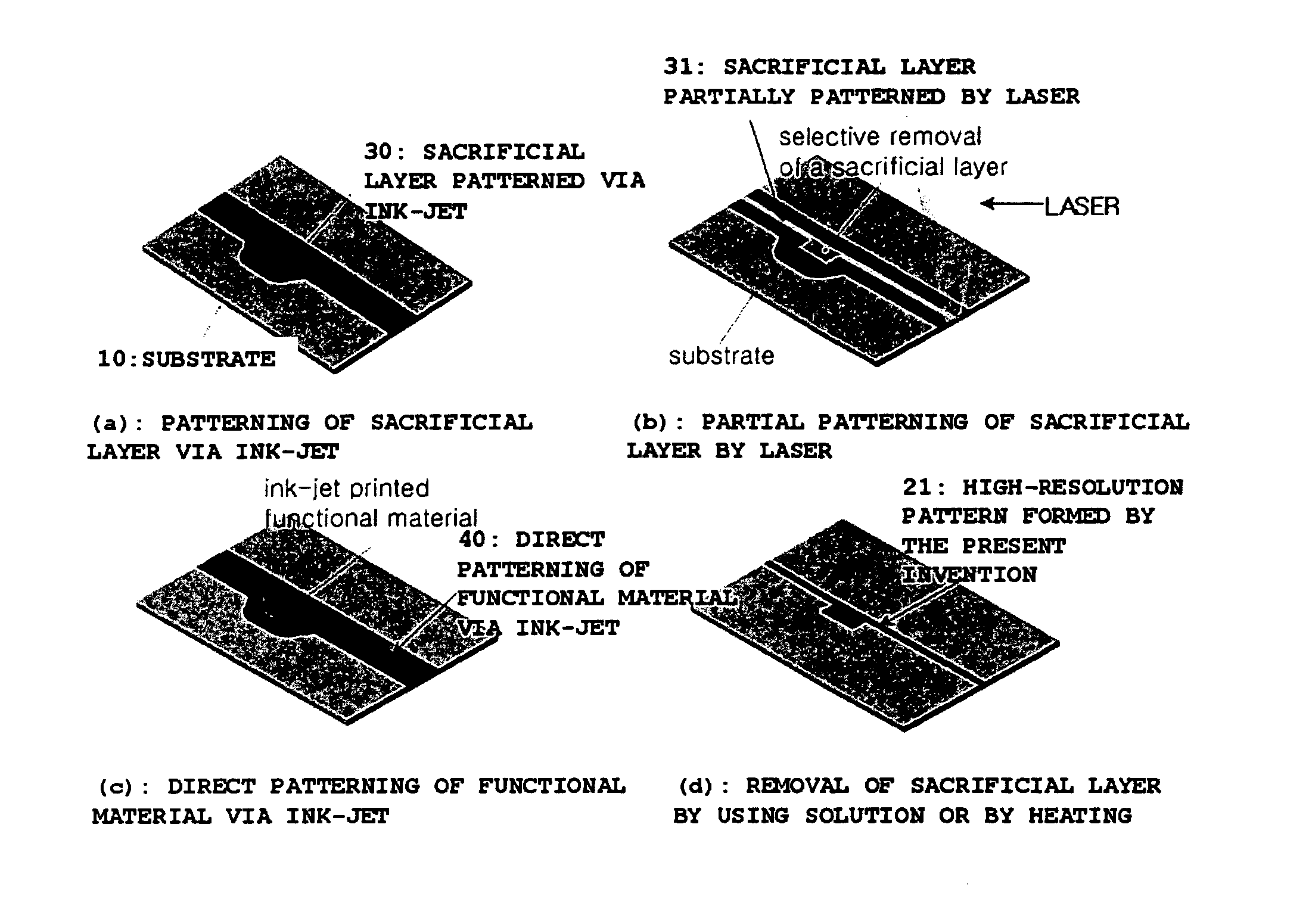
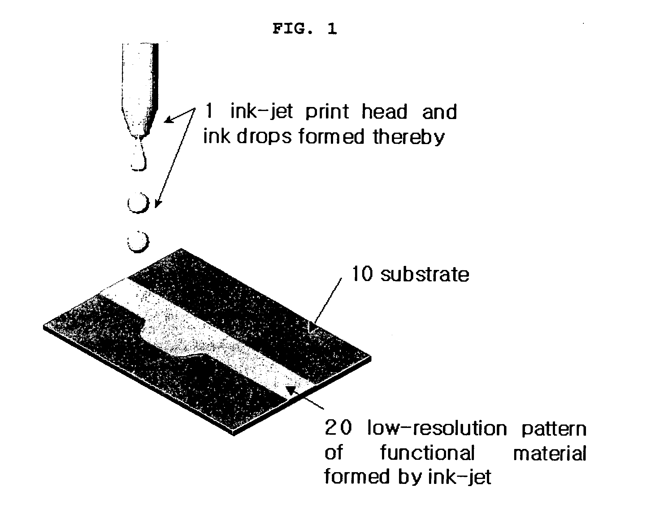
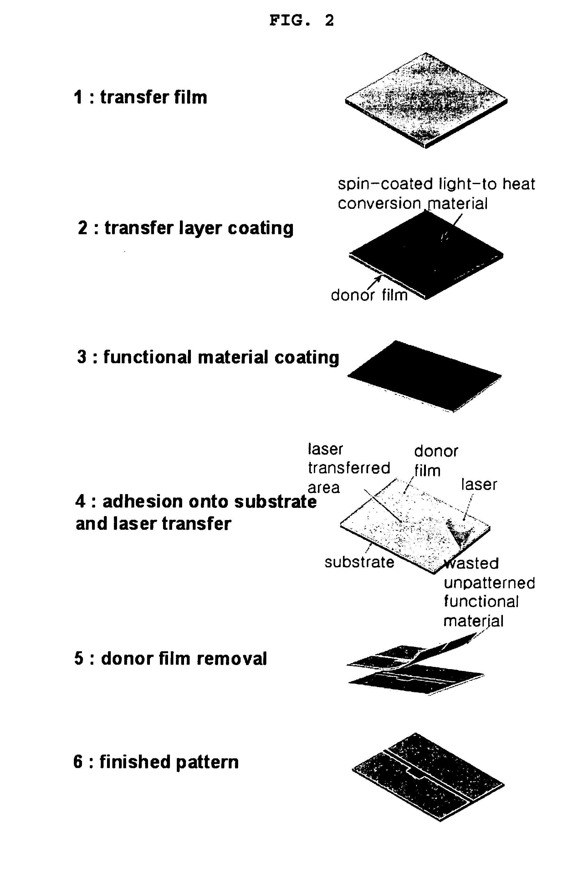
Method for forming high-resolution pattern with direct writing means
a high-resolution pattern and direct writing technology, applied in the field of high-resolution pattern and substrate, can solve the problems of wasteful photolithography, poor applicability of a new design of photolithography to actual production lines, poor processing efficiency, etc., and achieve low waste of high-cost functional materials. , the effect of high processing efficiency
- Summary
- Abstract
- Description
- Claims
- Application Information
AI Technical Summary
Benefits of technology
Problems solved by technology
Method used
Image

Examples
example 1
[0100] In this example, a non-polar material was used as functional material ink containing no particles dispersed therein, and a polar material was used as a sacrificial layer material to provide little or no solubility between the functional material and the sacrificial layer.
[0101] First, to provide a composition for forming a sacrificial layer, 1.5 g of polyvinylalcohol (weight average molecular weight: 7,200, Fluka, 81368) and 0.5 g of a UV absorbing agent (black dye, LC Chem.) were dissolved in 15 g of water, 1 g of ethyleneglycol, and 0.5 g of glycerol to form ink for ink-jet. Next, the ink is applied onto a glass substrate by using an ink-jet device (JetLab, MicroFab) to form the pattern of a sacrificial layer with a width of 600 μm. Then, the pattern of the sacrificial layer was partially removed by UV laser (355 nm, Avia 2000, Coherent Inc.) with a beam diameter of 30 μm to form regions to be patterned subsequently by a functional layer. The laser was operated under the c...
example 2
[0102] In this example, a polar material was used as functional material ink containing particles dispersed therein, and a non-polar material was used as a sacrificial layer material to provide little or no solubility between the functional material and the sacrificial layer.
[0103] First, to provide a composition for forming a sacrificial layer, 5 g of PMMA (weight average molecular weight: 50,000, Fluka, CAS No. 9011-14-7) and 1.5 g of a UV absorbing agent (black dye, LC Chem.) were dissolved in 1,2-Dichloroethane(Molecular weight: 98.96, CAS No. 107-06-2) to form ink for ink-jet. Next, the ink is applied onto a glass substrate by using an ink-jet device (JetLab, MicroFab) to form the pattern of a sacrificial layer with a width of 500 μm. Then, the pattern of the sacrificial layer was partially removed by UV laser (355 nm, Avia 2000, Coherent Inc.) with a beam diameter of 30 μM to form regions to be patterned subsequently by a functional layer. The laser was operated under the con...
PUM
 Abstract
Description
Claims
Application Information