Semiconductor device and driving method of the same

a technology of semiconductor devices and driving methods, applied in the direction of electronic switching, pulse techniques, instruments, etc., can solve the problems of source driver circuit problems, affecting and affecting the realization of large and high luminance displays, so as to reduce the effect of variations in transistor characteristics and improve the write speed of signals

Active Publication Date: 2006-12-21
SEMICON ENERGY LAB CO LTD
View PDF65 Cites 8 Cited by
  • Summary
  • Abstract
  • Description
  • Claims
  • Application Information

AI Technical Summary

Benefits of technology

[0048] According to the invention, in the case of supplying a current to a transistor of a pixel or a signal driver circuit, a precharge operation is performed in advance. Therefore, a write of current is terminated rapidly. Furthermore, as a period for performing the precharge operation is controlled appropriately, a current can be set accurately without waste. Moreover, rapid precharge can be achieved to obtain a predetermined potential. As a result, an effect of variations in characteristics of transistors can be reduced, a predetermined current can be supplied, and a write speed of a signal can be improved sufficiently independently of an amount of potential change of a signal line even with a small signal current.

Problems solved by technology

The former has a simple structure, but has a problem such that a realization of a large and high luminance display is difficult.
In the case of a display device of the active matrix method, there is a problem that a current flowing to a light emitting element varies due to a variation in current characteristics of driving TFTs, which varies a luminance.
The aforementioned examples relate to a technology for compensating a change of current due to variations of driving TFTs in pixel circuits, however, the same problem occurs in a source driver circuit as well.

Method used


Image

  • Semiconductor device and driving method of the same
  • Semiconductor device and driving method of the same
  • Semiconductor device and driving method of the same

Examples


embodiment mode 1

[0095] According to the invention, a pixel is formed of an element which is capable of controlling a luminance according to a current value supplied to a light emitting element. Typically, an EL element can be applied. Among various known structures of an EL element, any element structure can be applied to the invention as long as it can control a luminance by a current value. That is, an EL element is formed by freely combining a light emitting layer, a charge transporting layer, and a charge injection layer, for which materials can be selected from a low molecular weight organic material, medium molecular weight organic material (organic light emitting material having no sublimation property and of which number of molecules is 20 or less, or a length of chain molecules is 10 μm or less) or a high molecular weight organic material. Further, the aforementioned material mixed or dispersed with non-organic material may be used.

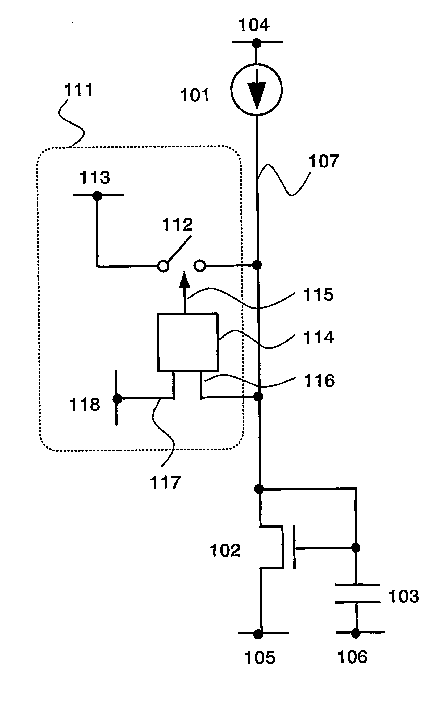
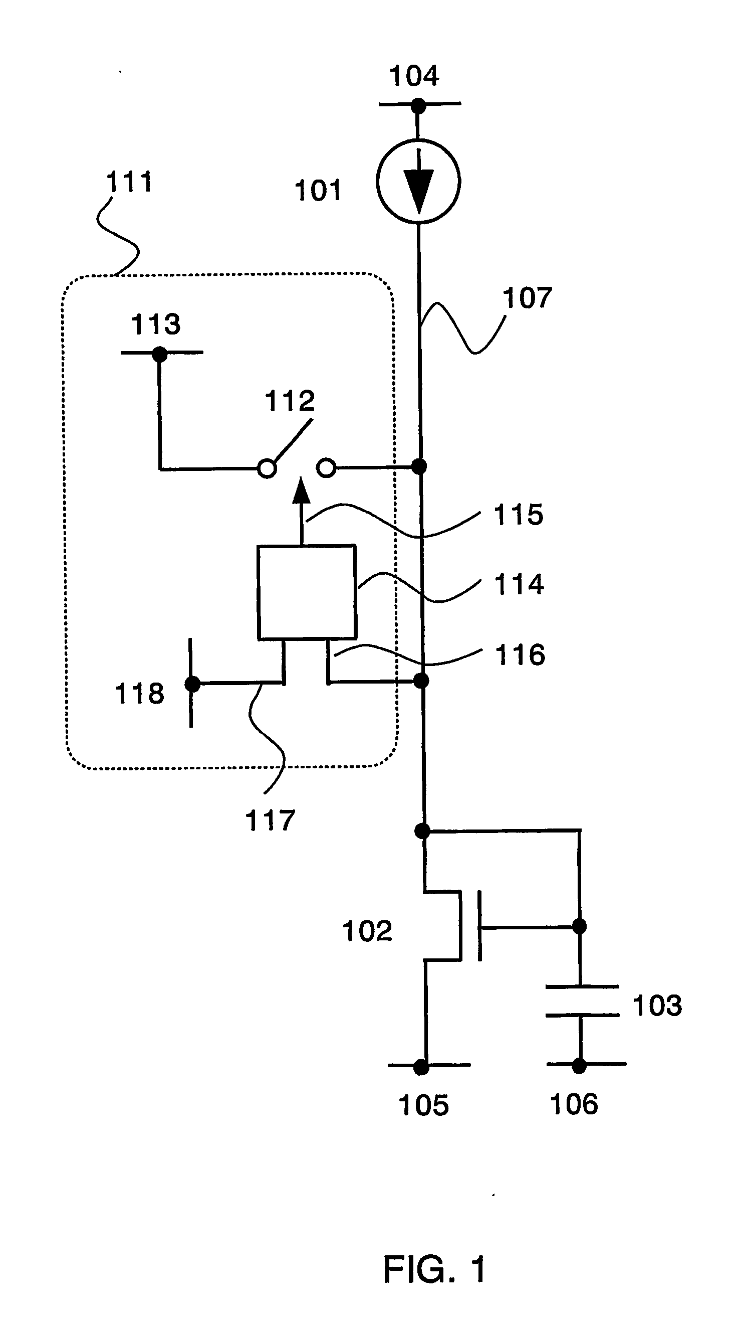
[0096] First, a configuration based on the basic principl...

embodiment mode 2

[0116] FlG. 8 shows the case where the initial potential of the wiring 107 is higher than a potential obtained in the steady state as the most typical case. However, the initial potential of the wiring 107 is practically lower than the potential in the steady state in some cases. Now, the case of performing a precharge regardless of high and low of the initial potential is described.

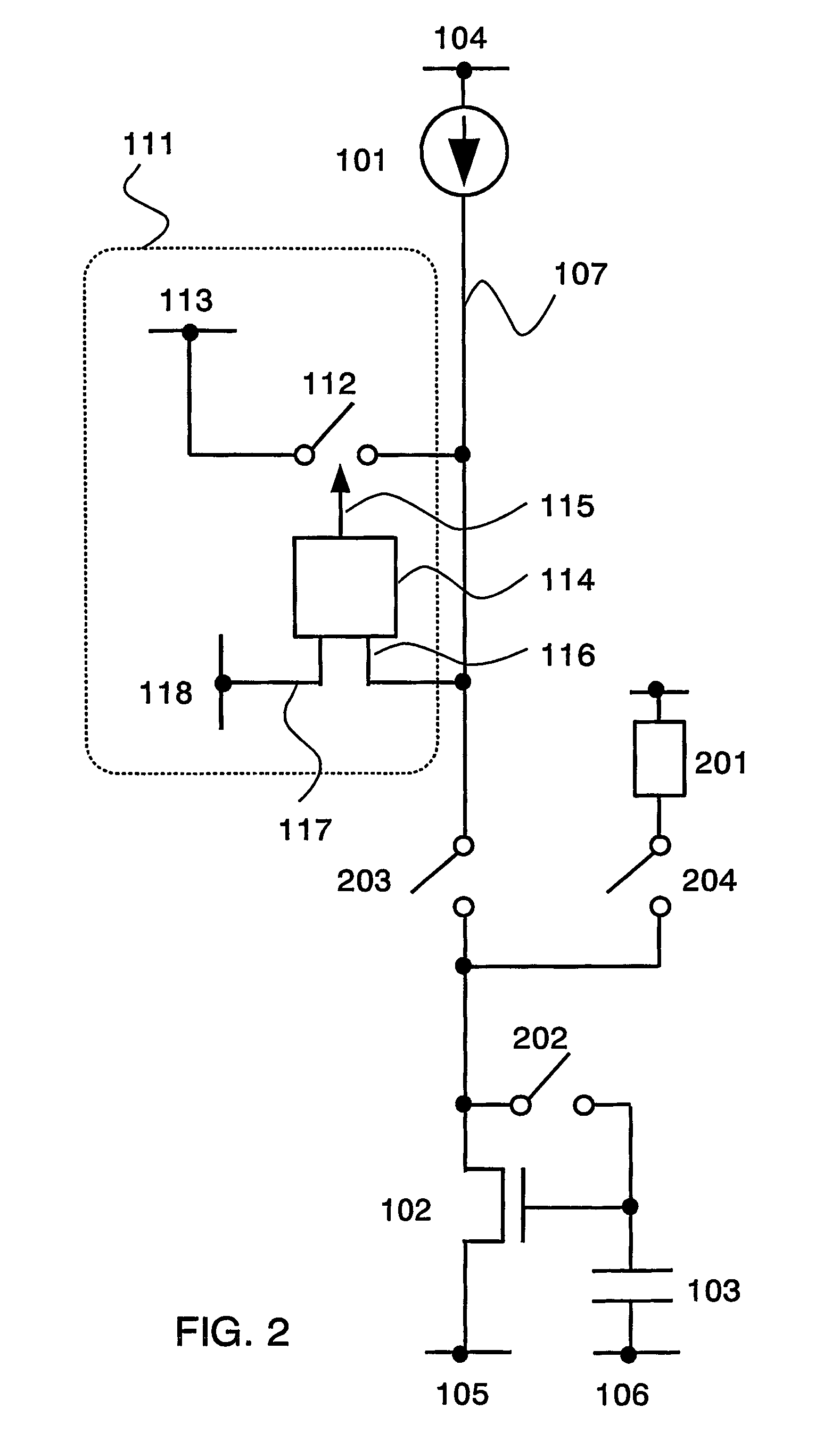
[0117] First, FIG. 14 shows the case of disposing a plurality of precharge circuits 111a and 111b as a configuration example. It is assumed that a potential of a wiring 113a is higher than a potential of a wiring 113b. Therefore, the wiring 113a may be connected to a wiring 104 while the wiring 113b may be connected to a wiring 105.

[0118] In the case where the potential of the wiring 107 is lower, the precharge switch 112a is turned ON and a charge is supplied from the wiring 113a, thereby the potential of the wiring 107 rises rapidly. Otherwise, in the case where the potential of the wiring 107 is hig...

embodiment mode 3

[0133] Next, a specific example of a comparison control circuit is described. First, FIG. 22 shows the case where a comparison control circuit is configured by using an operational amplifier 2214. In the case of FIG. 22, a non-inverting terminal is connected to the wiring 118 and an inverting terminal is connected to the wiring 107. Therefore, in the case where the potential of the wiring 107 is low, a potential of the output terminal 115 becomes high. In the case where a potential of the wiring 113 is high, a precharge may be performed when the potential of the wiring 107 is low. In that case, the switch 112 may be turned ON.

[0134] Note that in the case where the potential of the output terminal 115 is to be high when the potential of the wiring 107 is high, for example, an inverter may be connected to an end of an output of the operational amplifier 2214 as shown in FIG. 23 to invert data or a connection of the non-inverting terminal and the inverting terminal of the operational ...


PUM


Abstract

In the case of reducing an effect of variations in current characteristics of transistors by inputting a signal current to a transistor in a pixel, a potential of a wiring is detected by using a precharge circuit. In the case where there is a difference between a predetermined potential and the potential of the wiring, a charge is supplied to the wiring to perform a precharge by charging rapidly. When the potential of the wiring reaches the predetermined potential, the supply of charge is stopped and a signal current only is supplied. Thus, a precharge is performed only in a period until the potential of the wiring reaches the predetermined potential, therefore, a precharge can be performed for an optimal period.

Description

TECHNICAL FIELD [0001] The present invention relates to a semiconductor device provided with a function to control by a transistor a current to be supplied to a load. In particular, the invention relates to a pixel formed of a current drive type light emitting element of which luminance changes according to a current, a semiconductor device including a signal driver circuit which drives a pixel, and a driving method thereof. BACKGROUND ART [0002] In a display device using such a self-luminous light emitting element as OLED (Organic Light Emitting Diode), organic EL element and EL (Electro Luminescence) element, a passive matrix method and an active matrix method are known as its driving method. The former has a simple structure, but has a problem such that a realization of a large and high luminance display is difficult. Therefore, the active matrix method is developed in recent years in which a current flowing to the light emitting element is controlled by a thin film transistor (T...

Claims


Application Information

Patent Timeline
Patent Type & Authority Applications(United States)
IPC IPC(8): G09G3/30
CPCG09G3/3241G09G3/325G09G3/3275H03K17/16G09G2310/0248G09G2320/0219G09G2320/043G09G2300/0819G09G3/3266G09G3/3283H03K17/162
Inventor KIMURA, HAJIME
Owner SEMICON ENERGY LAB CO LTD
Why Eureka
Try Eureka