Methods of making templates for use in imprint lithography and related structures

a technology of imprint lithography and template, applied in the field of making templates for use in imprint lithography and related structures, can solve the problems of limited resolution of conventional photolithography, high cost of photolithographic equipment, and slow processing speed

Active Publication Date: 2006-12-21
MICRON TECH INC
View PDF14 Cites 72 Cited by
  • Summary
  • Abstract
  • Description
  • Claims
  • Application Information

AI Technical Summary

Benefits of technology

[0005] The present invention, in one exemplary embodiment, relates to a method of forming a template for use in imprint lithography that comprises providing an ultraviolet (“UV”) wavelength radiation transparent layer and forming a pattern in the UV wavelength radiation transparent layer by photolithography. The UV wavelength radiation transparent layer may comprise a UV wavelength radiation transparent material selected from the group consisting of quartz, magnesium fluoride, titanium oxide, calci...

Problems solved by technology

The limitations on the resolution of conventional photolithography are due to the wavelength of radiation used in the process.
In addition, photolithographic equipment becomes increasingly expensive as feature sizes become smaller.
However, electron beam lithography is expensive and very slow.
However, use of these techniques is undesirable because they are expensive and have low throughput.

Method used


Image

  • Methods of making templates for use in imprint lithography and related structures
  • Methods of making templates for use in imprint lithography and related structures
  • Methods of making templates for use in imprint lithography and related structures

Examples


Embodiment Construction

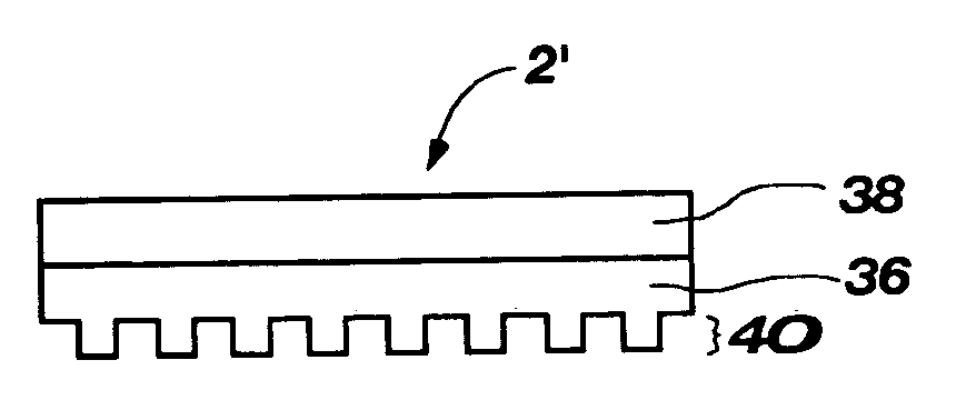
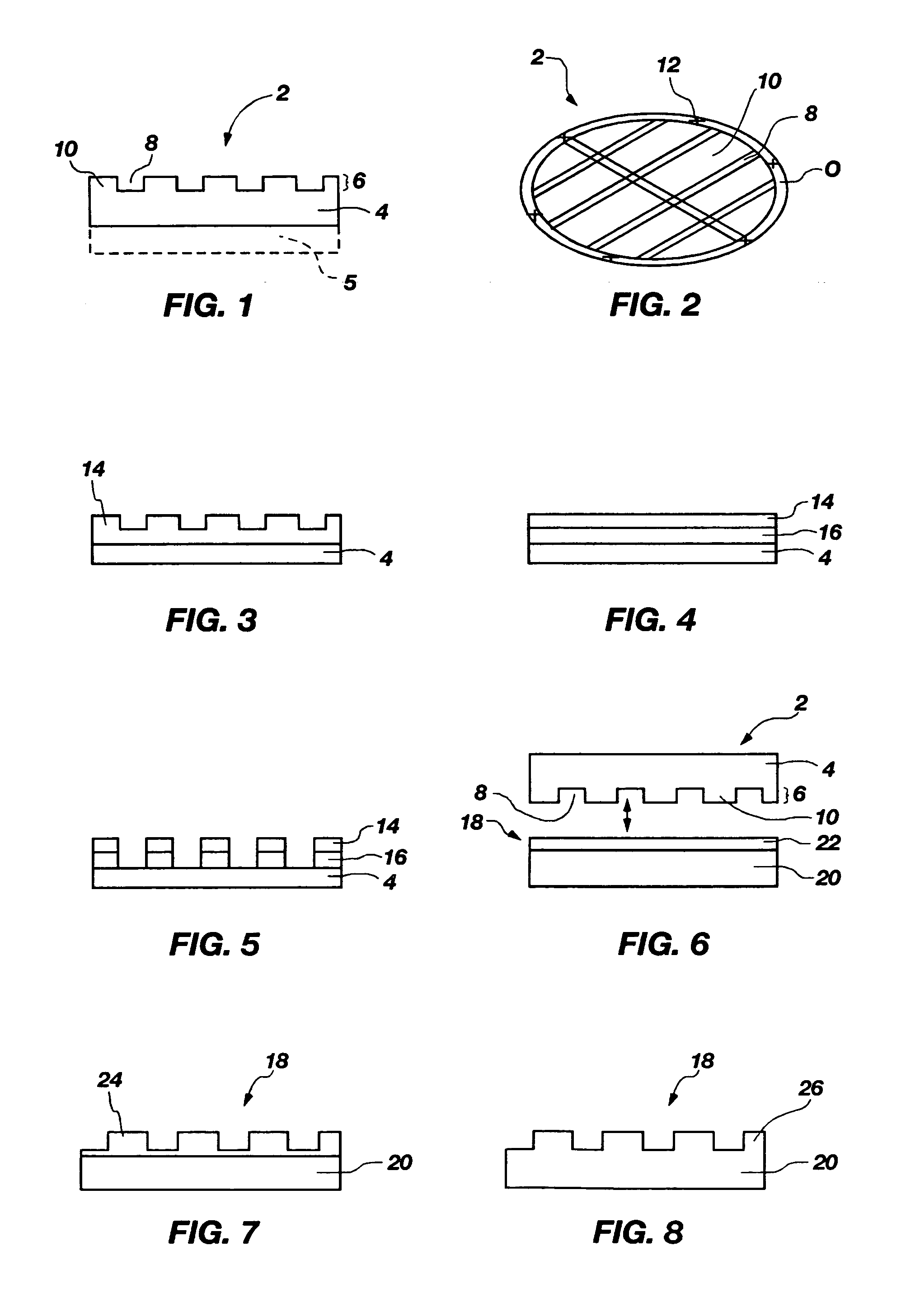
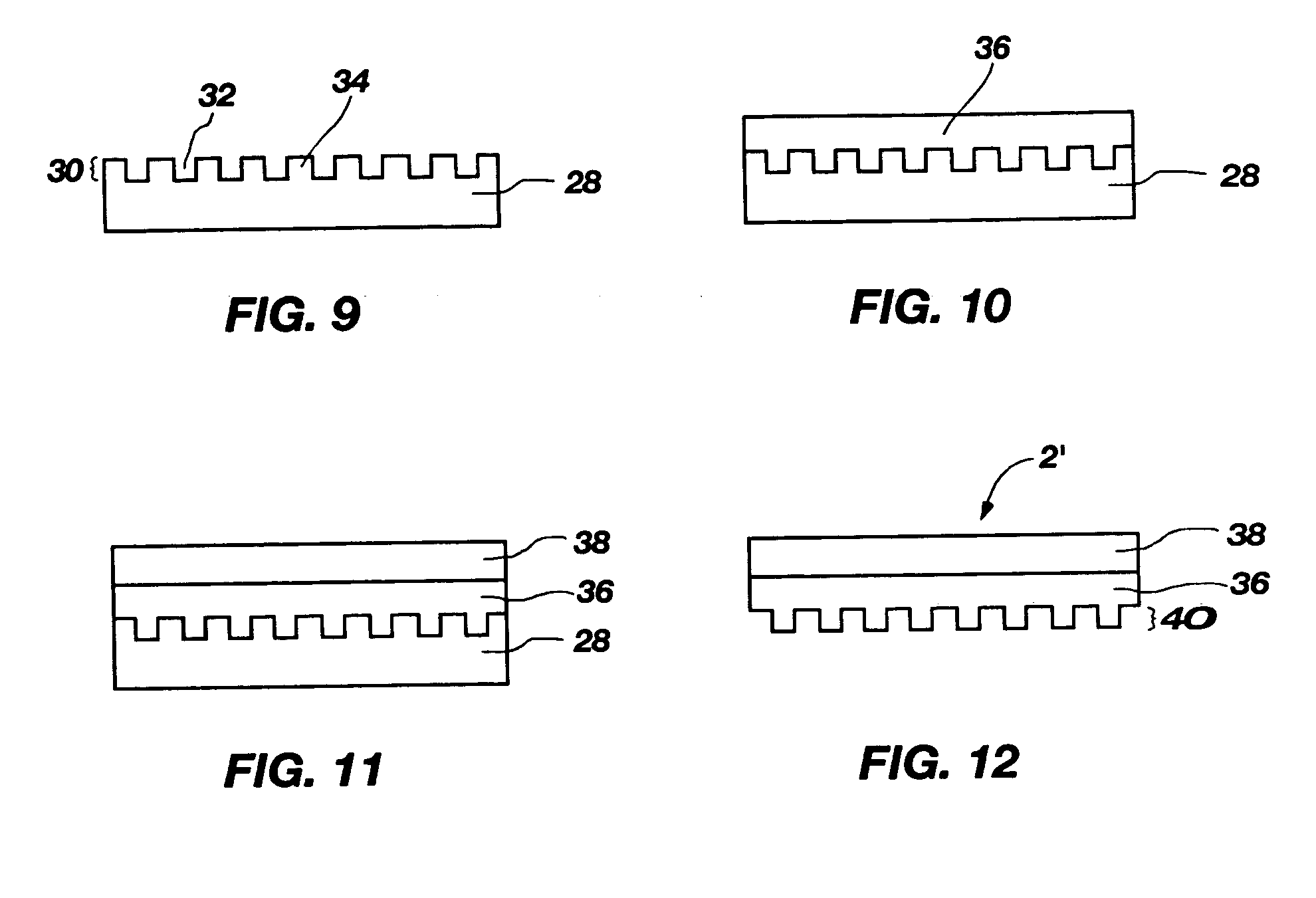
[0019] A template for use in imprint lithography is disclosed. The template includes a high resolution pattern that may be formed by lithography. The pattern on the template provides topography that is used to imprint a pattern of corresponding features on a semiconductor device. In other words, the template functions as a mold or form to transfer the pattern to the semiconductor device, forming the features on a surface thereof contacted by the template. As described in more detail below, the template may be transparent to UV wavelength radiation or may be opaque to UV wavelength radiation. The features on the semiconductor device may have dimensions substantially similar to dimensions of the pattern on the template. The features may have a feature size or dimension of less than approximately 100 nm, such as less than approximately 45 nm. By using photolithographic techniques to form the pattern, the template may be easily and cheaply fabricated. In addition, new infrastructure and...


PUM

PropertyMeasurementUnit
Nanoscale particle sizeaaaaaaaaaa
Wavelengthaaaaaaaaaa

Abstract

A method of forming a template for use in imprint lithography. The method comprises providing an ultraviolet (“UV”) wavelength radiation transparent layer and forming a pattern in the UV transparent layer by photolithography. The pattern may be formed by anisotropically etching the UV transparent layer and may have feature dimensions of less than approximately 100 nm, such as dimensions of less than approximately 45 nm. An additional embodiment of the method comprises providing a UV opaque layer comprising a first pattern therein, forming a first UV transparent layer in contact with the first contact-pattern of the UV opaque layer, forming a second UV transparent layer in contact with the first UV transparent layer, and removing the UV opaque layer to form the template. An intermediate template structure for use in imprint lithography is also disclosed. In other embodiments, a template that is opaque to UV wavelength radiation and a method of forming the same are disclosed.

Description

FIELD OF THE INVENTION [0001] The present invention relates to methods of fabricating templates for use in imprint lithography and related structures. More specifically, the present invention relates to fabricating such templates using photolithographic techniques. BACKGROUND OF THE INVENTION [0002] In the semiconductor industry, conventional patterning processes include patterning a photoresist layer by lithographic methods, such as photolithography, electron beam, or X-ray lithography, for mask definition. The pattern on the photoresist layer is subsequently transferred into a hard material in contact with the photoresist layer using a dry etch, wet etch, or lift-off technique. Photolithography is limited to forming features of approximately 90 nm with a 248 nm light, approximately 45 nm with a 193 nm light, and from approximately 25 nm to approximately 30 nm with a 13.7 nm (extreme ultraviolet (“EUV”)) light. The limitations on the resolution of conventional photolithography are ...

Claims


Application Information

Patent Timeline
IPC IPC(8): G03C5/00G03F9/00
CPCB82Y10/00B82Y40/00B29C59/16G03F7/0017G03F7/0002
Inventor SANDHU, GURTEJ S.RERICHA, WILLIAM T.
Owner MICRON TECH INC
Why Eureka
Try Eureka