Barrier-metal-free copper damascene technology using atomic hydrogen enhanced reflow

a damascene and copper technology, applied in the direction of semiconductor devices, semiconductor/solid-state device details, electrical apparatus, etc., can solve the problems of significant electrical resistance impact, achieve greater conductivity, lower resistivity, and high purity copper contacts

Inactive Publication Date: 2006-12-28
CONVERSANT INTPROP MANAGEMENT INC
View PDF36 Cites 14 Cited by
  • Summary
  • Abstract
  • Description
  • Claims
  • Application Information

AI Technical Summary

Benefits of technology

[0013] In another embodiment, the method can be used to form a dual damascene conductive structure in a semiconductor device by providing a substrate comprising a semiconductor component and an insulating layer over the semiconductor component, and etching the insulating layer to form a channel corresponding to a trench along the insulating layer, and an opening extending from the trench to the semiconductor component. A non-metal barrier layer is formed over the insulating layer including the exposed surface of the channel and the opening, and a conductive material is deposited on the barrier layer by ionized magnetron sputtering to fill the channel and the opening to form dual damascene conductive structures in the insulating layer. The dual damascene structures resulting from the process comprise an interconnect line coupled to a conductive contact to the semiconductor component. The barrier layer prevents diffusion of the copper into the insulating layer.
[0017] Advantageously, the present invention provides higher purity copper contacts and interconnects having a lower resistivity (greater conductivity) compared to prior art copper films and contact structures. The method advantageously eliminates void formation in sub-micron trenches and contact openings, and other high aspect ratio conductive features. The process also eliminates the need to form a separate diffusion barrier by transforming a portion of the insulating layer to form a diffusion barrier film or layer between the metal (copper) contact / interconnect and the insulating layer.

Problems solved by technology

However, copper atoms can easily diffuse through most oxides into the devices in the underlying silicon substrate and act as recombination centers to spoil device performance.
If the barrier thickness does not scale with the device (and wiring scaling), the impact on electrical resistance is significant.

Method used


Image

  • Barrier-metal-free copper damascene technology using atomic hydrogen enhanced reflow
  • Barrier-metal-free copper damascene technology using atomic hydrogen enhanced reflow
  • Barrier-metal-free copper damascene technology using atomic hydrogen enhanced reflow

Examples


Embodiment Construction

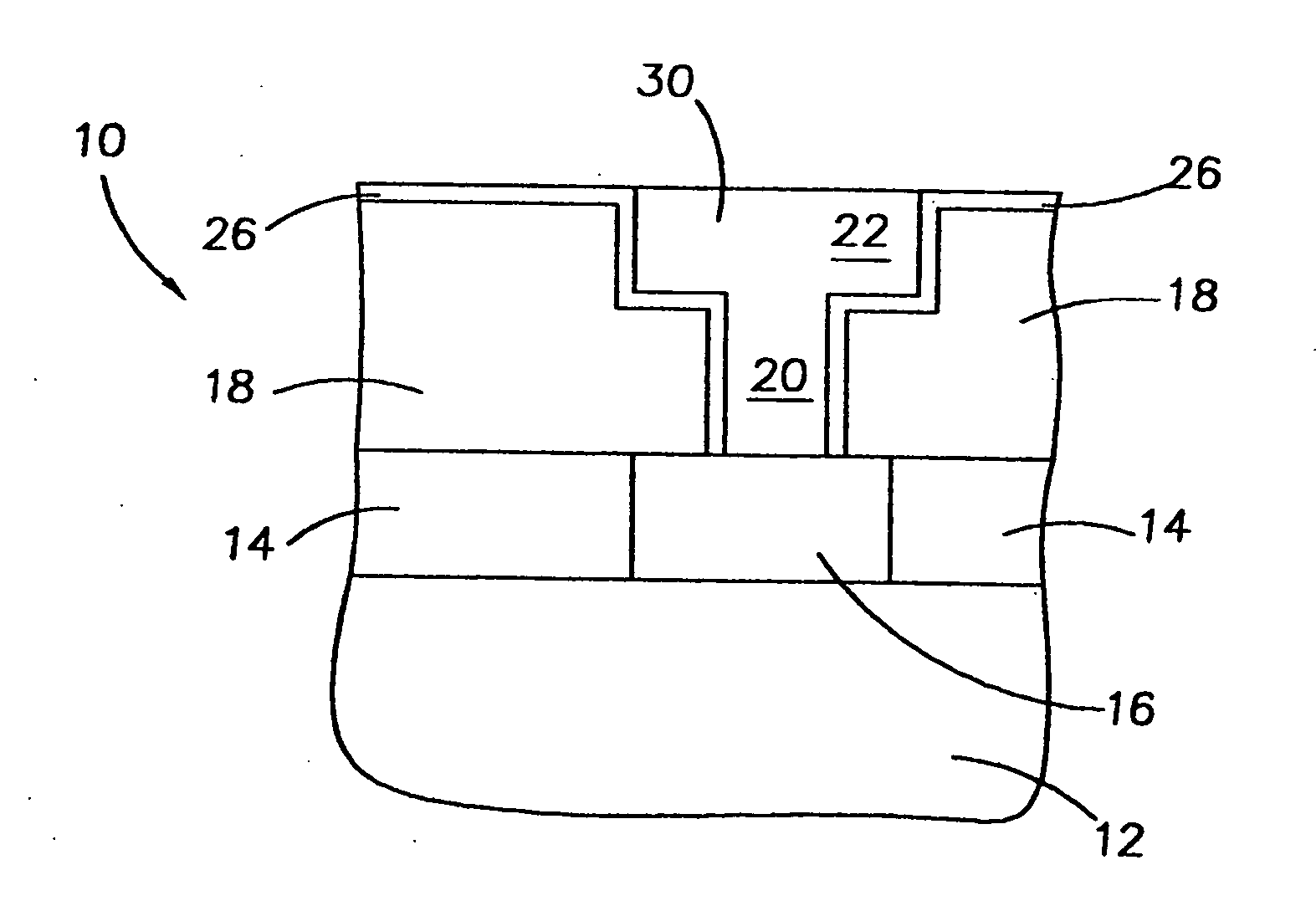
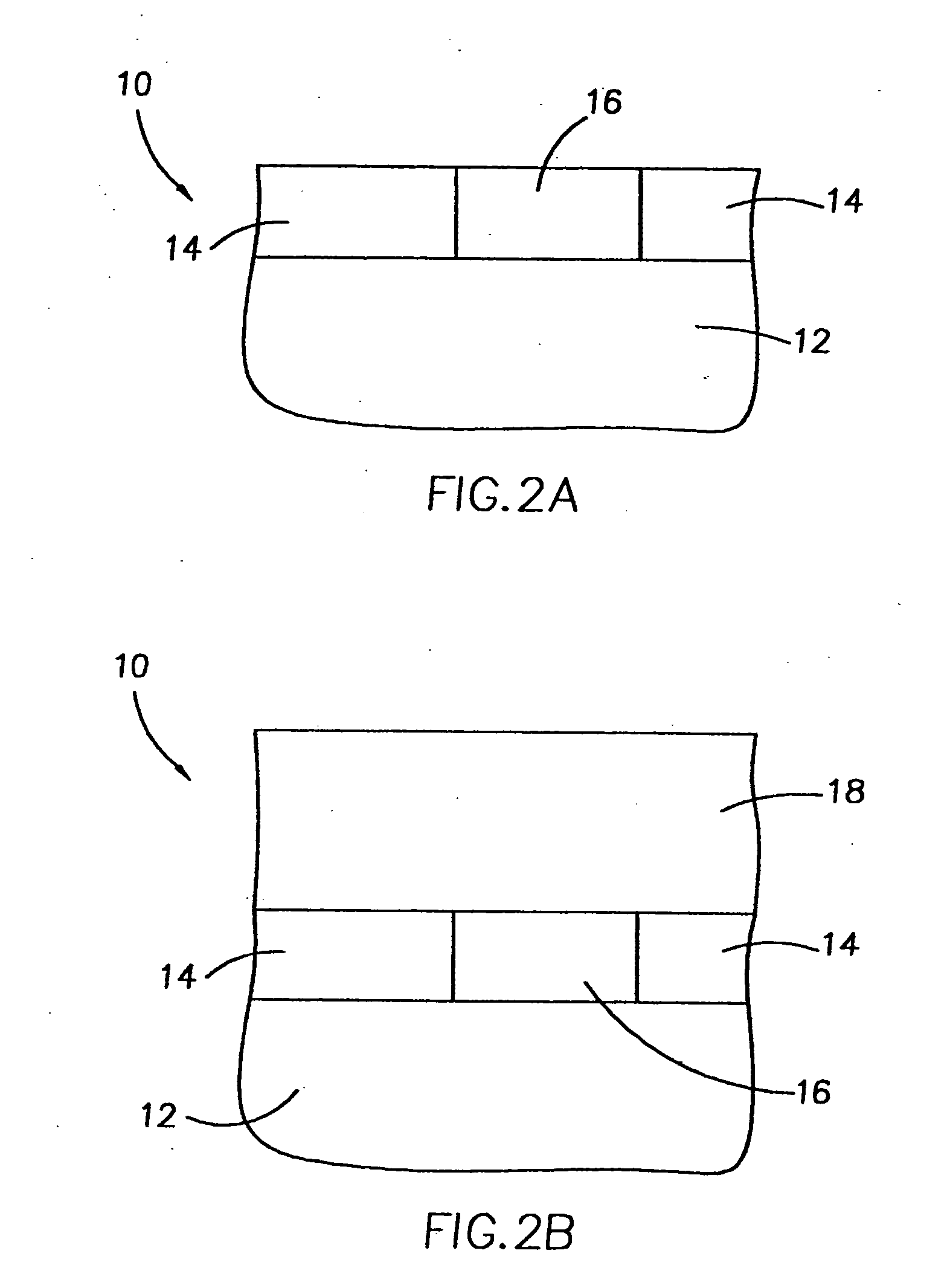
[0022] The present invention encompasses methods of making integrated circuits, particularly methods for forming copper contacts and interconnects using a dual damascene process.

[0023] The method of the invention will be described generally with reference to the drawings for the purpose of illustrating the present preferred embodiments of the invention only and not for purposes of limiting the same. The figures illustrate processing steps for use in the fabrication of semiconductor devices in accordance with the present invention. It should be readily apparent that the processing steps are only a portion of the entire fabrication process. The present invention particularly deals with the method of fabricating contacts and interconnects that are used in the fabrication of semiconductor devices.

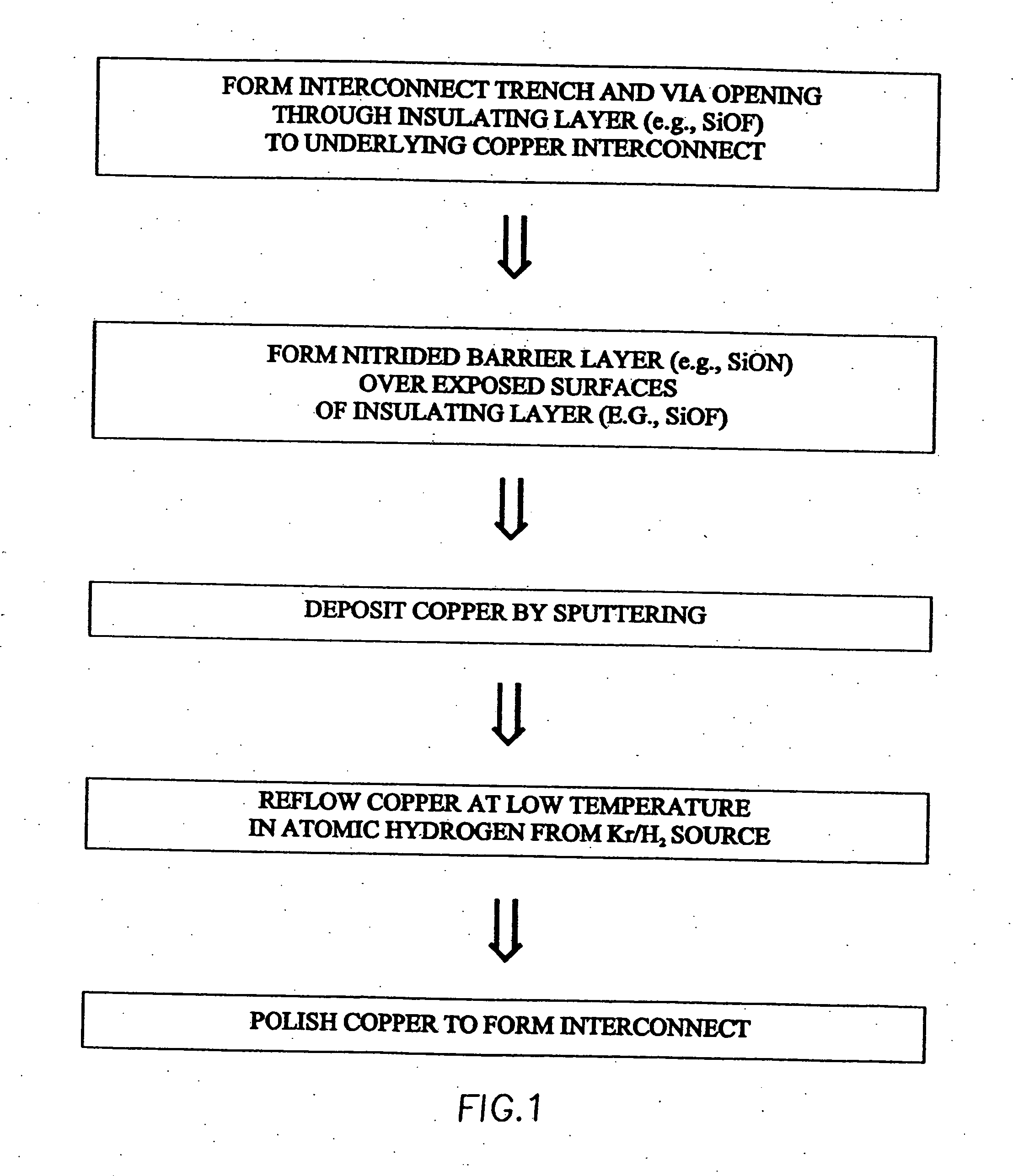
[0024]FIG. 1 provides a process flow diagram for a first embodiment of the method of the present invention. A semiconductor device is provided that has been processed to where a first level o...


PUM

PropertyMeasurementUnit
temperatureaaaaaaaaaa
thicknessaaaaaaaaaa
thicknessaaaaaaaaaa

Abstract

A method for forming conductive contacts and interconnects in a semiconductor structure, and the resulting conductive components are provided. In particular, the method is used to fabricate single or dual damascene copper contacts and interconnects in integrated circuits such as memory devices and microprocessor.

Description

CROSS REFERENCE TO RELATED APPLICATION [0001] The present application is a division of U.S. patent application Ser. No. 10 / 889,203, filed on Jul. 12, 2004, presently pending, which is a continuation of U.S. patent application Ser. No. 10 / 122,870, filed on Apr. 15, 2002, now U.S. Pat. No. 6,762,500, which is a division of U.S. patent application Ser. No. 09 / 809,670, filed Mar. 15, 2001, now U.S. Pat. No. 6,696,360.FIELD OF THE INVENTION [0002] The invention relates generally to semiconductor devices, and more particularly to interconnections within semiconductor circuits and methods of making the interconnections, including methods for fabricating copper interconnects. BACKGROUND OF THE INVENTION [0003] Integrated circuits are interconnected networks of resistors, transistors and other electrical components that are generally formed on a silicon substrate or wafer with conductive, insulative and semiconductive materials. Fabricating integrated circuits involves forming electrical com...

Claims


Application Information

Patent Timeline
Patent Type & Authority Applications(United States)
IPC IPC(8): H01L23/52H01L23/48H01L21/285H01L21/314H01L21/316H01L21/768
CPCH01L21/2855H01L21/3144H01L21/31629H01L21/76807H01L21/76814H01L21/76826H01L2924/0002H01L21/76831H01L21/76882H01L2924/00H01L21/3105H01L21/02332H01L21/0234
Inventor AHN, KIE Y.FORBES, LEONARD
Owner CONVERSANT INTPROP MANAGEMENT INC
Why Eureka
Try Eureka