Method of making a metal gate semiconductor device

a metal gate and semiconductor technology, applied in the field of integrated circuits, can solve the problems of polysilicon compatibility problems, difficult to find metals with work functions that work, and difficulty in etching these metals

Inactive Publication Date: 2006-12-28
NXP USA INC
View PDF3 Cites 69 Cited by
  • Summary
  • Abstract
  • Description
  • Claims
  • Application Information

AI Technical Summary

Problems solved by technology

Further, polysilicon has compatibility issues with many of the high k dielectrics being considered for use.
In the implementation of metal gates, much of the difficulty has been finding metals with work functions that work well for N channel and P channel transistors.
Etching these metals is also an issue.
The integration of the various aspects of choosing the metals for P and N channel devices, the gate dielectric, and the etchants has been difficult to achieve for reliable manufacturing.

Method used


Image

  • Method of making a metal gate semiconductor device
  • Method of making a metal gate semiconductor device
  • Method of making a metal gate semiconductor device

Examples


Embodiment Construction

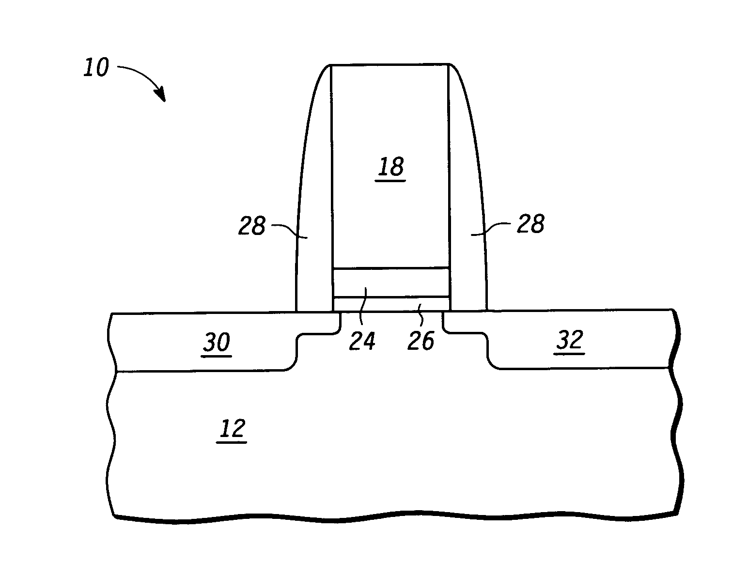
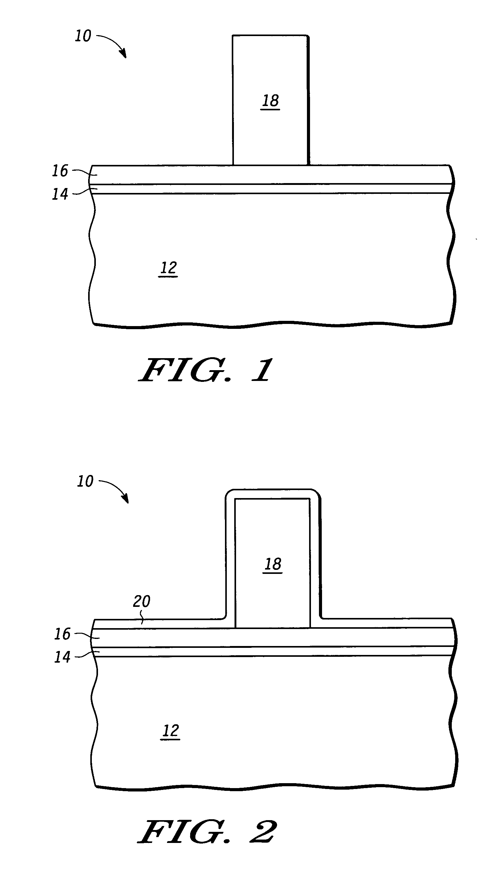
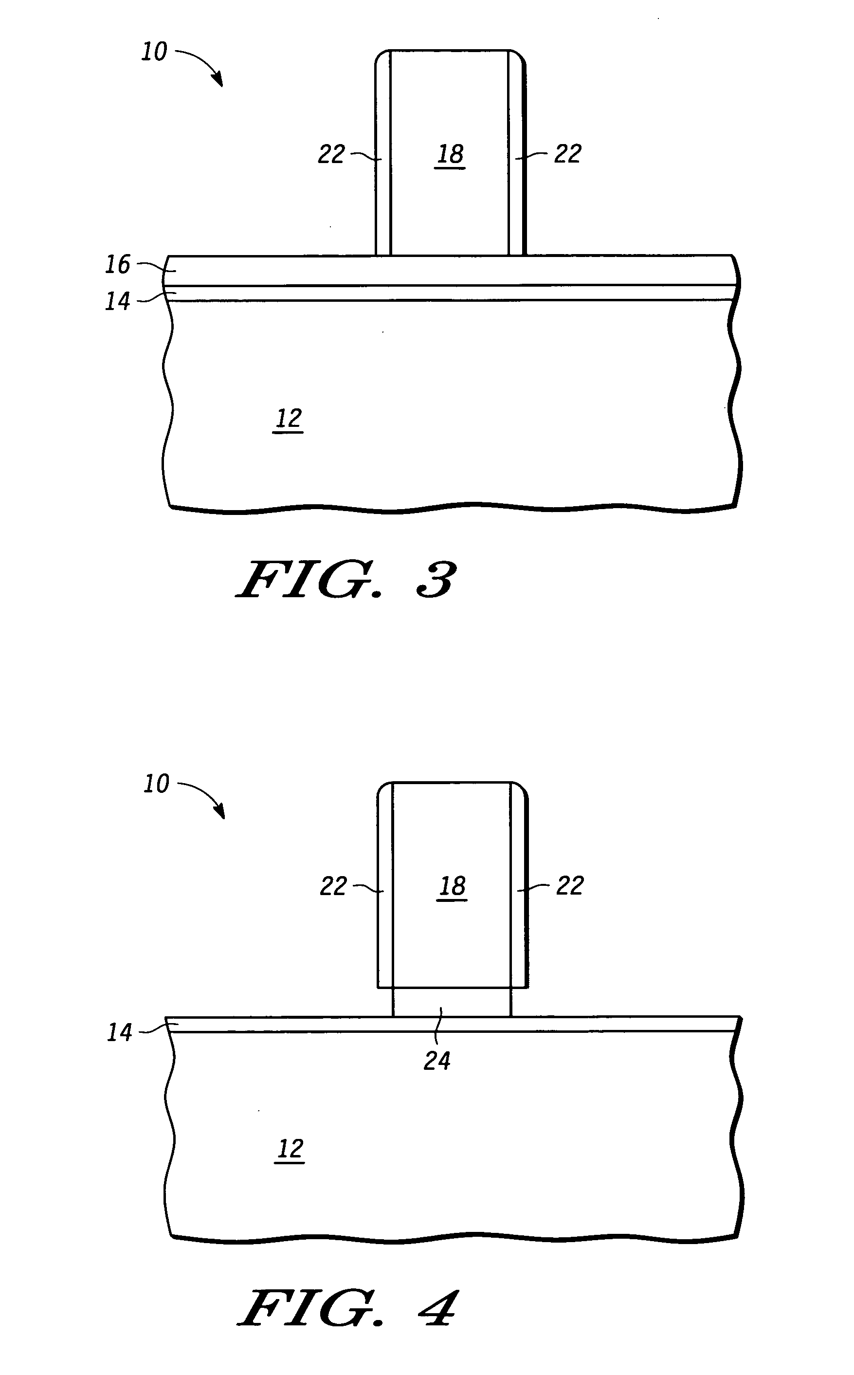
[0012] In one aspect a semiconductor device has a patterned polysilicon gate over a metal layer that is over a gate dielectric layer, which in turn is over a semiconductor substrate. A thin layer of material, preferably the same material as the gate dielectric, is conformally deposited over the polysilicon gate and over the exposed metal layer. The conformal layer is etched back to form a sidewall spacer on the polysilicon gate and to re-expose the previously exposed portion of the metal layer. The re-exposed metal layer is etched using an etchant that is selective to the gate dielectric material and the sidewall spacer. Even though this etch is substantially anisotropic, it has an isotropic component that would adversely etch the sidewall of the polysilicon gate but for the protection provided by the sidewall spacer. After the re-exposed metal has been removed, a transistor is formed in which the gate is a stack of the polysilicon gate and the unetched portion of the metal layer. T...


PUM

PropertyMeasurementUnit
thicknessaaaaaaaaaa
thickaaaaaaaaaa
thickaaaaaaaaaa

Abstract

A patterned polysilicon gate is over a metal layer that is over a gate dielectric layer, which in turn is over a semiconductor substrate. A thin layer of material is conformally deposited over the polysilicon gate and the exposed metal layer and then etched back to form a sidewall spacer on the polysilicon gate and to re-expose the previously exposed portion of the metal layer. The re-exposed metal layer is etched using an etchant that is selective to the gate dielectric material and the sidewall spacer. Even though this etch is substantially anisotropic, it has an isotropic component that would etch the sidewall of the polysilicon gate but for the protection provided by the sidewall spacer. After the re-exposed metal has been removed, a transistor is formed in which the metal layer sets the work function of the gate of the transistor.

Description

FIELD OF THE INVENTION [0001] This invention relates to integrated circuits, and more particularly to forming a semiconductor device having a metal gate. BACKGROUND OF THE INVENTION [0002] Polysilicon has been the gate of choice for MOS transistors for many years. As the gate dielectrics have become thinner and / or of a higher dielectric constant (k), depletion (poly depletion) of carriers in the polysilicon adjacent to the gate dielectric, which has the effect of adding a capacitor in series with the gate dielectric, has become more significant in reducing the overall gate capacitance. A typical effect of poly depletion is to put the equivalent of 6 to 8 Angstroms of silicon oxide in series with the gate dielectric. With gate dielectrics now being able to be made with equivalents of about 10 Angstroms of silicon oxide, the poly depletion is significant to the effective overall gate dielectric thickness as measured electrically. With the improved use of high k dielectrics, the poly d...

Claims


Application Information

Patent Timeline
Patent Type & Authority Applications(United States)
IPC IPC(8): H01L21/336
CPCH01L29/4966H01L29/7833H01L29/6659H01L29/517
Inventor GOOLSBY, BRIAN J.WHITE, BRUCE E.
Owner NXP USA INC
Why Eureka
Try Eureka