Dressing tool, dressing device, dressing method, processing device and semiconductor device producing method

a dressing device and dressing surface technology, applied in the direction of grinding/polishing apparatus, grinding machine components, grinding/polishing machines, etc., can solve the problems of uneven deterioration of the construction of the dressing apparatus, imbalance of the contact surface pressure between the dressing surface, etc., to ensure the flatness of the polishing surface of the polishing pad, and high degree of precision

Inactive Publication Date: 2006-12-28
NIKON CORP
View PDF8 Cites 3 Cited by
  • Summary
  • Abstract
  • Description
  • Claims
  • Application Information

AI Technical Summary

Benefits of technology

[0015] Secondly, it is an object of the present invention to provide a dressing tool which can ensure the flatness of the polishing surface of the polishing pad following dressing with a high degree of precision, and a dressing apparatus using this dressing tool.
[0016] Third, it is an object of the present invention to provide a dressing method and apparatus which can dress a polishing pad to a flat surface with a higher degree of precision, to provide a polishing apparatus which can polish an object of polishing using this polishing pad that has been dressed to a flat surface with a high degree of precision, and to provide a semiconductor device manufacturing method which makes it possible to manufacture semiconductor devices at a higher yield and lower cost than conventional semiconductor device manufacturing methods.

Problems solved by technology

Working tools that perform polishing, grinding or lapping, etc., deteriorate due to the fact that clogging of the working surface progresses as the working time increases.
Furthermore, the following problem also arises: namely, in order to cause uniform contact of the dressing surface 111 of the rotating dressing tool 110 with the pad surface 101 of the polishing pad 100 that is thus rotating, either the polishing pad 100 or the dressing tool 110 must be centered by means of a gimbal centering mechanism, etc., so that the construction of the dressing apparatus tends to become complicated.
Furthermore, even if support by means of a centering mechanism is thus provided, if the dressing tool 110 deviates toward the outer circumferential side or inner circumferential side of the pad surface 101, there is a resulting imbalance in the contact surface pressure between the dressing surface 111 and pad surface 101, so that there is a problem in terms of a loss of flatness of the pad surface 101 following dressing.
However, in the case of the above-mentioned conventional dressing tools, it is difficult to flatten the polishing surface of the polishing pad with a high degree of precision.
As a result of such a low flatness of the polishing pad, it is difficult to polish semiconductor wafers, etc., to a flat surface with a high degree of precision using such a polishing pad.
Furthermore, dressing is performed by causing contact between the polishing surface of the polishing pad supported on a substrate and the dressing surface of the dressing tool, and causing relative motion between the above-mentioned substrate and dressing tool.
Because of manufacturing error, etc., it is difficult to position the rotational axis of the above-mentioned substrate and the rotation axis of the dressing tool so that these axes are perfectly parallel; accordingly, the two rotational axes are actually slightly inclined relative to each other.

Method used


Image

  • Dressing tool, dressing device, dressing method, processing device and semiconductor device producing method
  • Dressing tool, dressing device, dressing method, processing device and semiconductor device producing method
  • Dressing tool, dressing device, dressing method, processing device and semiconductor device producing method

Examples


Embodiment Construction

[0064] Preferred working configurations of the present invention will be described below with reference to the figures. However, the descriptions of these working configurations do not limit the scope of the present invention.

[First Working Configuration]

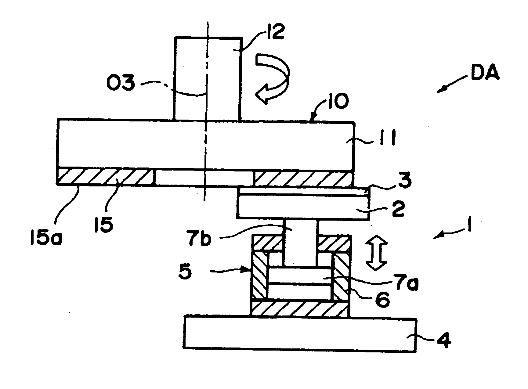
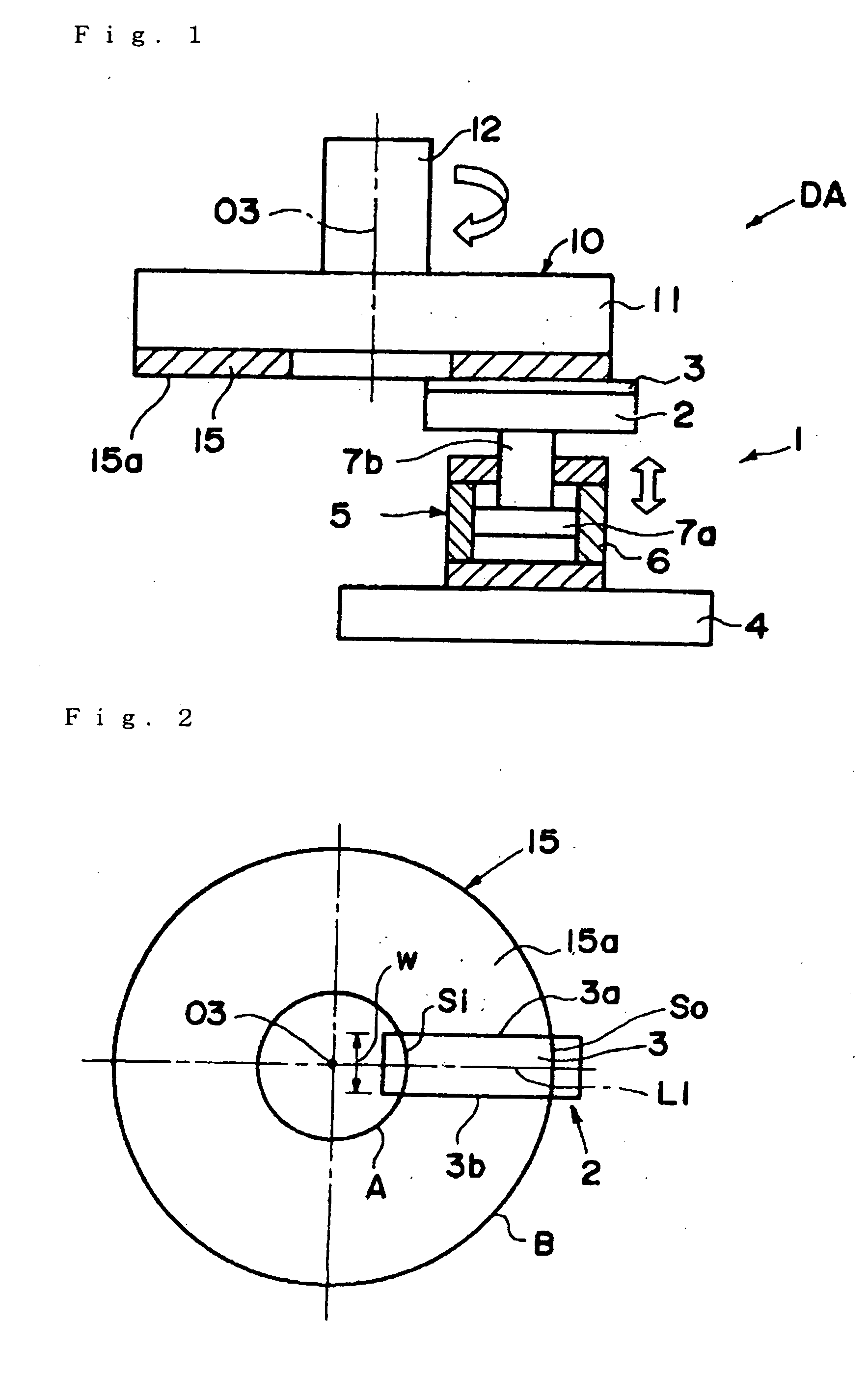
[0065] A dressing apparatus DA for a polishing pad constructed using the dressing tool 2 of the present invention is shown in FIG. 1. This dressing apparatus DA is an apparatus which dresses a pad surface (polishing surface) 15a of a polishing pad 15 used in a CMP apparatus, and is constructed from a pad holding mechanism 10 which holds the polishing pad 15 by vacuum chucking, etc., and causes this polishing pad 15 to rotate, and a dressing tool holding mechanism 1 which has a dressing tool 2 that dresses the pad surface 15a of the polishing pad 15 that is held and caused to rotate by the above-mentioned pad holding mechanism 10. The pad holding mechanism 10 is constructed from a pad holding head 11 which holds the polishing pad 1...


PUM

PropertyMeasurementUnit
DAaaaaaaaaaa
external diameteraaaaaaaaaa

Abstract

A dressing apparatus DA is constructed from a pad holding mechanism 10 which holds a polishing pad 15 that has a doughnut disk-form pad surface 15a, and which causes this polishing pad 15 to rotate, a dressing tool 2 which has a substantially rectangular dressing surface 3, and a dressing tool holding mechanism 1 which holds the dressing tool 2 so that the dressing surface 3 of this dressing tool 2 is caused to face the pad surface 15a of the polishing pad 15 that is held and caused to rotate by the pad holding mechanism 10. The dressing tool holding mechanism 1 causes the held dressing tool 2 to contact the pad surface 15a in a state in which the centerline L1 in the direction of width of the dressing surface 3 is oriented so that this centerline extends in the radial direction of the pad surface 15a, and thus causes dressing to be performed. As a result, the flatness of the working surface following dressing can be improved.

Description

[0001] The present application is a continuation of PCT International Application No. PCT / JP02 / 09022 filed on Sep. 5, 2002, which is hereby incorporated by reference.TECHNICAL FIELD [0002] The present invention relates to a dressing tool, a dressing apparatus and a dressing method which are used to dress the working surface of a working tool that is used to perform polishing, grinding or lapping, etc., a working apparatus which has such a dressing tool or dressing apparatus, and a semiconductor device manufacturing method. BACKGROUND ART [0003] Working tools that perform polishing, grinding or lapping, etc., deteriorate due to the fact that clogging of the working surface progresses as the working time increases. Accordingly, such working tools are maintained by performing periodic dressing so that favorable working can always be performed. For example, such working tools include polishing pads that are used in chemical-mechanical polishing apparatuses (CMP apparatuses) that perform...

Claims


Application Information

Patent Timeline
Patent Type & Authority Applications(United States)
IPC IPC(8): B24B1/00B24B21/18B24B53/007B24B53/017
CPCB24B53/017B24B53/12
Inventor HOSHINO, SUSUMUYAMAMOTO, EIICHI
Owner NIKON CORP
Why Eureka
Try Eureka