Semiconductor device and package, and method of manufacturer therefor

a technology of semiconductor devices and semiconductor devices, applied in the field of semiconductor devices, can solve the problems of difficulty in downsizing the package, limited number of leads that can be provided for the package, and various problems of conventional semiconductor devices related to soldering, and achieve the effect of easy detection

Inactive Publication Date: 2007-01-04
YAMAHA CORP
View PDF2 Cites 19 Cited by
  • Summary
  • Abstract
  • Description
  • Claims
  • Application Information

AI Technical Summary

Benefits of technology

[0017] It is another object of the invention to provide a method of manufacturing semiconductor packages with a high reliability.
[0018] It is a further object of the invention to provide a semiconductor device and a manufacturing method therefor in which the prescribed amount of solder can be constantly supplied to electrode surfaces of terminals so as to avoid formation of solder bridges between adjoining terminals, wherein the semiconductor device provides a sufficient resistance against separation between the terminals and the package, regardless of any impact that may occur when removing the terminal support portion by dicing or by a pull-up operation for pulling up the semiconductor device after connection with the external circuit.
[0021] A semiconductor device is produced using a package in which a semiconductor chip mounting on a stage and terminals are embedded within a resin. Herein, pads of the semiconductor chip are respectively connected with terminals by fine lines. Each of the terminals can be modified in structure and configuration. That is, an interconnecting portion like a flange is arranged inside of the resin package at the prescribed elevation above the electrode surface that is exposed on the mounting surface. The interconnecting portion is horizontally elongated so that one terminal surface thereof is exposed to the cut surface, which corresponds to the side wall of the package or the side wall of the dicing groove. In particular, an isolation portion is formed as an integral part of the package made by the resin and is arranged in the prescribed area between the electrode surface and the exposed terminal surface of the interconnecting portion with respect to each terminal. Due to the provision of the isolation portion, it is possible to stabilize amounts of solder adhered to the electrode surfaces. In addition, it is possible to avoid unwanted formation of a solder bridge between the electrode terminal and exposed terminal surface. Further, it is possible to secure a sufficient resistance against the separation of the terminal being peeled off from the package, regardless of any impact that occurs when terminal supports of the frame are cut out and a pull-up operation for pulling up the semiconductor device after connection with the external circuit.
[0022] Specifically, it is preferable that the thickness of the isolation portion range from 25% to 75% as compared to the overall thickness of the terminal at its electrode surface. Due to the provision of the isolation portion of adequate size, it is possible to reliably prevent the solder from flowing from the electrode surface to the exposed terminal surface. Hence, it is possible to reliably avoid unwanted formation of a solder bridge between them. The isolation portion is continuously formed as an integral part of the package and is formed to continuously cover the terminal surface between the electrode surface and the exposed terminal surface. For this reason, if the thickness of the isolation portion is less than 25% of the overall thickness of the terminal, the isolation portion may be easily destroyed when a certain tension stress is imparted to the terminal. Hence, it may be impossible to provide sufficient strength for resisting the separation of the terminal from the package. On the other hand, if the thickness of the isolation portion exceeds 75% of the overall thickness of the terminal, the thickness of the interconnecting portion becomes extremely small due to the drawing process for drawing the interconnecting portion deep into the package by etching or polishing. This would result in the unwanted reduction in the strength of the terminal.
[0024] Moreover, at least one electrode surface can be partially deformed to provide a distinction from the other ‘normal’ electrode surfaces that are arranged on the mounting surface. Alternatively, it is possible to provide an asymmetric arrangement for the electrode surfaces on the mounting surface. Thus, a human operator or optical reader can easily detect the direction of the semiconductor device to be connected with the external circuit.

Problems solved by technology

However, the number of leads that can be provided for the package must be limited by the resin sealed area representing the prescribed portion of the package sealed within the resin.
In order to secure the necessary number of leads, it is necessary to enlarge the resin sealed area, which may create difficulty in downsizing of the package.
However, the conventional semiconductor devices have various problems related to soldering.
In other words, this may cause deviations for joint strengths in the connection with the external circuit.
In addition, the unstable consumption of solder may cause troubles for the production management of semiconductor devices.
A further problem related to soldering is that when the semiconductor device is pulled up as shown in FIG. 27C after connected with the external circuit, the terminals 202 may be easily separated or isolated from the package 104.
However, this structure does not eliminate the continuation between the exposed terminal surface and electrode surface of the terminal 210.
As a result, the aforementioned publication does not provide effective solutions for the aforementioned problems caused by deviations in the amounts of solder fillets F being adhered to the terminals and by formation of a bridge between the adjoining terminals.
Due to such insufficient joint force, when the semiconductor device is pulled up after connected with the external circuit, it could not avoid the separation between the terminals 210 and the package 104.

Method used


Image

  • Semiconductor device and package, and method of manufacturer therefor
  • Semiconductor device and package, and method of manufacturer therefor
  • Semiconductor device and package, and method of manufacturer therefor

Examples


first embodiment

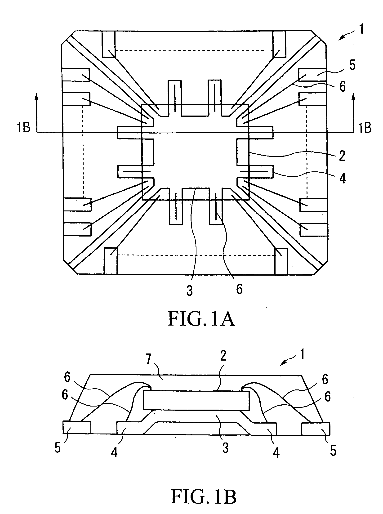
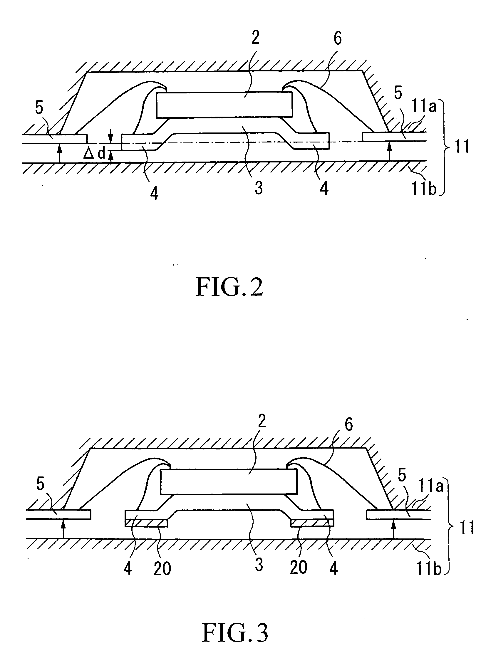
[0061]FIGS. 1A and 1B show the structure and internal configuration of a semiconductor package 1 in accordance with a first embodiment of the invention. Specifically, FIG. 1A is a plan view showing the upper appearance of the semiconductor package 1; and FIG. 1B is a sectional view of the semiconductor package 1 taken along line 1B-1B in FIG. 1A.

[0062] Reference numeral 2 designates a semiconductor chip, which is supported by a stage 3. Reference numeral 4 designate inner leads that are arranged in the periphery of the stage 3; and reference numeral 5 designate outer leads that are arranged in the outer periphery of the semiconductor package 1 in its bottom. The inner leads 4 and the outer leads 5 are electrically connected together with bonding pads on the semiconductor chip 2 via metal fine lines 6. The aforementioned semiconductor chip 2, stage 3, inner leads 4, and outer leads 5 are all enclosed or sealed within a resin 7, together forming the package 1.

[0063] Compared to the ...

second embodiment

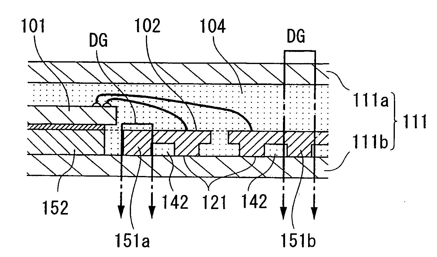
[0078]FIG. 4 is a sectional view showing selected parts of a semiconductor device in accordance with a second embodiment of the invention. FIG. 5 is a plan view showing an appearance of the semiconductor device that is viewed from its backside (or mounting surface), wherein electrode surfaces are formed to establish connections using external lines.

[0079] In the semiconductor device of the second embodiment, pads 101a of a semiconductor chip 101 are electrically connected to terminals 102 via fine lines 103. Herein, the terminals 102 contain inner terminals 102a and outer terminals 102b, which are respectively aligned in an inner line and an outer line in the periphery of a package 104. Both the inner terminal 102a and outer terminal 102b provide electrode surfaces 121, which are exposed externally. The aforementioned elements such as the semiconductor chip 101 and terminals 102 are enclosed or sealed within the package 104 that is composed of a thermosetting resin compound (herein...

third embodiment

[0095] Next, a semiconductor device of a third embodiment of the invention will be described with reference to FIG. 12, wherein the third embodiment is substantially similar to the foregoing second embodiment except for the designated structure for the lead frame 105. Hence, the third embodiment is described with respect to only the structure of the frame 105.

[0096]FIG. 12 is a plan view showing the appearance of one unit of the frame 105, which is viewed from its mounting surface and is used to manufacture the semiconductor device of the third embodiment. Actually, as has been described above numerous units of the frames 105 are horizontally arranged and interconnected together.

[0097] In FIG. 12, the lead frame 105 is made by a metal plate having a substantially externally rectangular shape. A stage 152 for mounting a semiconductor chip 101 is formed substantially at the center of the ‘rectangular’ frame 105. A pair of terminal supports 151a, each of which connects together the p...


PUM


Abstract

A semiconductor package encapsulating a semiconductor chip provides inner leads and outer leads for establishing electrical connections with the substrate. Herein, a lead frame is set into the metal mold, into which a resin is injected and which is clamped in proximity to the outer leads. Thus, the semiconductor package is sealed so as to avoid unwanted formation of resin burrs around lower surfaces of the inner leads. In addition, a semiconductor device is produced using a package in which a semiconductor chip mounted on a stage and terminals are embedded within a resin. Each terminal provides an electrode surface, an interconnecting portion, and an exposed terminal surface. Herein, an isolation portion is formed as an integral part of the package made by the resin and is arranged in the prescribed area between the electrode surface and the exposed terminal surface.

Description

CROSS-REFERENCE TO RELATED APPLICATION [0001] This application is a continuation under 35 U.S.C. §120 of U.S. application Ser. No. 10 / 120,391, filed Apr. 12, 2002, the entirety of which is incorporated by reference herein.BACKGROUND OF THE INVENTION [0002] 1. Field of the Invention [0003] This invention relates to semiconductor devices that provide semiconductor chips and components encapsulated in packages by resins. This invention also relates to methods of manufacturing semiconductor devices and packages. [0004] 2. Description of the Related Art [0005] Recent progresses of electronic and information technologies provide a variety of electronic devices that use considerable numbers of semiconductor components installed therein in a highly concentrated manner. This brings a strong demand to downsize packages for encapsulating semiconductor components and chips in resins. Conventionally, so-called QFN packages (namely, quad flatpack non-leaded packages) are used to realize the downs...

Claims


Application Information

Patent Timeline
Patent Type & Authority Applications(United States)
IPC IPC(8): H01L21/00H01L23/495H01L23/50H01L21/56H01L23/31
CPCH01L21/565H01L23/3107H01L2924/014H01L2924/01023H01L24/48H01L2924/01082H01L2924/01078H01L2924/01047H01L2924/01033H01L23/49503H01L23/49551H01L24/49H01L2224/32014H01L2224/48091H01L2224/48247H01L2224/48257H01L2224/49171H01L2224/49175H01L2924/01002H01L2924/01005H01L2924/01006H01L2924/01027H01L2924/00014H01L2924/00H01L2924/181H01L2224/45099H01L2224/05599H01L2924/00012H01L23/50
Inventor SHIRASAKA, KENICHISAITOH, HIROSHI
Owner YAMAHA CORP
Why Eureka
Try Eureka