Electronic device and driving method thereof

a technology of electronic devices and driving methods, applied in static indicating devices, instruments, optics, etc., can solve the problems of limited ability to make multiple gray scales, difficult to increase resolution, and difficult to make a lot of gray scales, and achieve high duty ratio

Inactive Publication Date: 2007-01-11
SEMICON ENERGY LAB CO LTD
View PDF37 Cites 17 Cited by
  • Summary
  • Abstract
  • Description
  • Claims
  • Application Information

AI Technical Summary

Benefits of technology

[0034] An object of the present invention is therefore to provide a novel method of driving, in which a high duty ratio is maintained in an electronic device performing driving as stated above, which is capable of normally performing display of an image even for cases having a sustain (turn on) period shorter than the above stated minimum unit, and which is capable of handling cases in which problems such as the above stated shift in the threshold value develop.
[0038] The voltage between a gate and a source of an EL driver TFT 102 in the state that the reset TFT 105 is made conductive can be controlled by changing the electric potential of the gate signal line 106 with the present invention. In accordance with this type of method, even if the threshold voltage of the EL driver TFT 102 is shifted, becoming a normally ON state, the EL driver TFT 102 can be placed in a non-conductive state with certainty by changing the electric potential of the gate signal line 106. It therefore becomes possible to make it difficult for electric current to flow in an EL element 103.

Problems solved by technology

Disadvantages of this method include fact that it is difficult to increase the resolution, and fact that it is difficult to make a lot of gray scales, because the number of sub-pixels cannot be made large without limits.
Problems such as the following appear, however, when the address (write in) periods and the sustain (turn on) periods are not separated.
The ability to make multiple gray scales is therefore limited by the minimum unit of the sustain (turn on) period.
The lengths of the sustain (turn on) periods for cases in which the digital gray scale method is combined with the time gray scale method are therefore determined by ratios of powers of 2, and considering the length of one frame period, it becomes difficult to realize multiple gray scales.
A problem in which the minimum unit of the sustain (turn on) period is limited for cases in which the address (write in) period and the sustain (turn on) period are not separated is stated in the above timing charts.
Gate signal lines of differing columns are selected at the same time with this type of overlap portion, and therefore normal scanning cannot be performed.
However, when using a pixel like that shown in FIGS. 17A and 17B, problems such as the following exist.
There are cases in which this varying deterioration and manufacturing irregularities become causes for a shift of the threshold voltage to a positive number.
This cannot be handled even if the electric potential of each signal line is changed.

Method used


Image

  • Electronic device and driving method thereof
  • Electronic device and driving method thereof
  • Electronic device and driving method thereof

Examples


embodiment 1

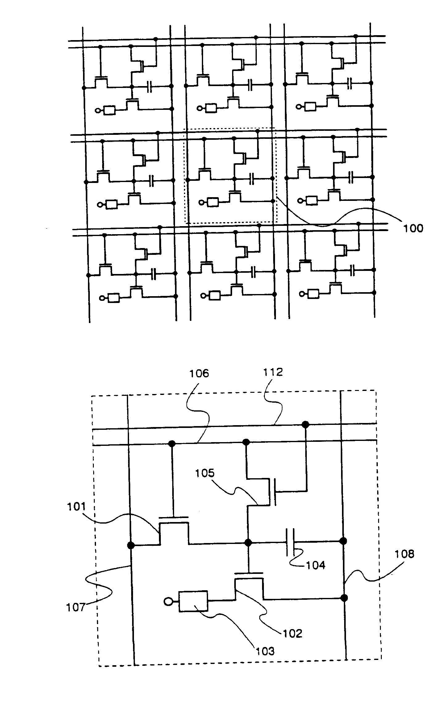
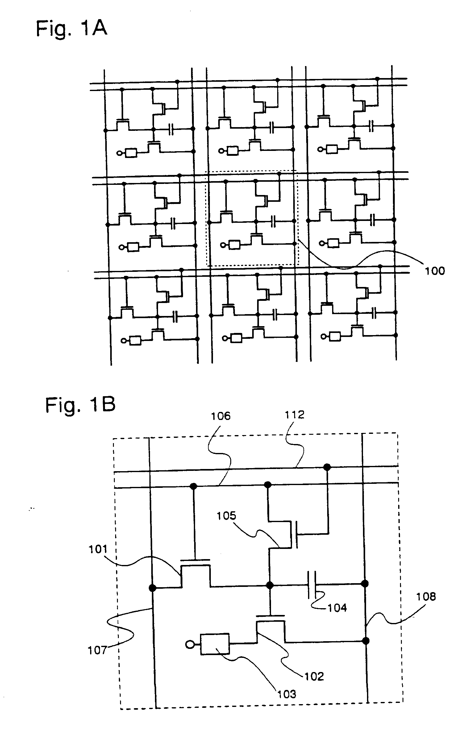
[0120]FIG. 3A is an example of an entire circuit structure of an electronic device shown by Embodiment 1. A pixel portion 351 is arranged in the center of a substrate 350. A source signal line driver circuit 352 is arranged on the top side of the pixel portion 351 in order to control source signal lines. To the left side of the pixel portion 351 is arranged a gate signal line driver circuit 353 in order to control gate signal lines. A reset signal line driver circuit 354 is arranged on the right side of the pixel portion 351 in order to control reset signal lines. A portion surrounded by a dotted line frame 300 in the pixel portion 351 is one pixel portion circuit, and an enlargement diagram is shown in FIG. 3B. The names of respective portions of FIG. 3B are similar to those of FIG. 1B, and therefore are omitted here.

[0121] Actual driving is discussed next. In Embodiment 1, k-bit (2k) gray scales are expressed by a method in which digital gray scales and time gray scales are combi...

embodiment 2

[0131] In Embodiment 2, a detailed description will be made of a method of simultaneously manufacturing, on the same substrate, a pixel portion and a driver circuit TFT (N-channel type and P-channel type) formed in the periphery of the pixel portion is explained.

[0132] First, as shown in FIG. 6A, a base film 5002 made of an insulating film such as a silicon oxide film, a silicon nitride film or a silicon oxynitride film is formed on a substrate 5001 made from glass such as a barium borosilicate glass or an alumino borosilicate glass, typically #7059 glass or #1737 glass of Corning Corp. For example, a silicon oxynitride film 5002a formed from SiH4, NH3, N2O by a plasma CVD method with a thickness of 10 to 200 nm (preferably 50 to 100 nm), and a silicon oxynitride hydride film 5002b formed from SiH4 and N2O, similarly, with a thickness of 50 to 200 nm (preferably 100 to 150 nm) are laminated. In Embodiment 2, the base film 5002 is shown as a two-layer structure, but a single layer o...

embodiment 3

[0172] An example of manufacturing an electric device using the present invention is explained in embodiment 3.

[0173]FIG. 9A is a top view of an electric device using the present invention. FIG. 9B illustrates a cross-sectional view taken along the line X-X′ in FIG. 9A. In FIG. 9A, reference numeral 4001 is a substrate, reference numeral 4002 is a pixel portion, reference numeral 4003 is a source signal side driver circuit, and reference numeral 4004 is a gate signal side driver circuit. The driver circuits are connected to external equipment, through an FPC 4008, via wirings 4005 to 4007.

[0174] A covering material 4009, an airtight sealing material 4010 and a sealing material (also referred to as a housing material) 4011 (shown in FIG. 9B) are formed so as to enclose at least the pixel portion, preferably both the driver circuits and the pixel portion, at this point.

[0175] Further, FIG. 9B is a cross sectional structure of the electric device of the present invention. A driver c...


PUM


Abstract

A pixel is provided in which normal display of an image is possible even if a sustain period is shorter than an address period in a driving method combining digital gray scales and time gray scales, and in which operation can be compensated by changing the electric potential of a signal line even for a case in which the EL driver transistor becomes normally on due to deterioration. One of a source region and a drain region of an erasure TFT is connected to an electric current supply line, and the remaining one of the source region and the drain region is connected to a gate signal line. It is possible to change the voltage between a gate and a source of an EL driver TFT by changing the electric potential of the gate signal line so that the EL driver TFT is placed in a non-conducting state with certainty with this structure, even for cases in which the EL driver TFT becomes normally on due to a shift in the value of its threshold voltage.

Description

BACKGROUND OF THE INVENTION [0001] 1. Field of the Invention [0002] The present invention relates to an electronic device structure. In particular, the present invention relates to an active matrix electronic device having a thin film transistor (TFT) formed on an insulating body, and to a method of driving an active matrix electronic device. [0003] 2. Description of the Related Art [0004] EL displays (also referred to as electroluminescence displays) have been gathering attention in recent years as flat panel displays, which are substitutes for LCDs (liquid crystal displays), and research into such displays is proceeding apace. [0005] LCDs can roughly be divided into two types of driving methods. One is a passive matrix type used in an LCD such as an STN-LCD, and the other is an active matrix type used in an LCD such as a TFT-LCD. EL displays can also be similarly broken down roughly into two types. One is a passive matrix type, and the other is an active matrix type. [0006] For th...

Claims


Application Information

Patent Timeline
Patent Type & Authority Applications(United States)
IPC IPC(8): G09G3/36G09G3/20G09G3/32H05B44/00
CPCG09G3/3659G09G3/3258G09G2300/0842G09G2300/0861G09G2310/0251G09G2310/0254G09G2310/061G09G2320/043H01L27/1214H01L29/42384H01L29/4908H01L29/78621H01L29/78627G09G3/2018G09G3/2022G09G3/2074G09G3/3233G09G2300/0426H01L27/1255H01L27/124G09G3/30G02F1/133
Inventor KIMURA, HAJIME
Owner SEMICON ENERGY LAB CO LTD
Why Eureka
Try Eureka