Method and system for performing local geometrical operation on a hierarchical layout of a semiconductor device

Inactive Publication Date: 2007-01-11
INFINEON TECH AG
View PDF2 Cites 22 Cited by
  • Summary
  • Abstract
  • Description
  • Claims
  • Application Information

AI Technical Summary

Benefits of technology

[0020] In various aspects, the current invention is concerned with a method and a system in

Problems solved by technology

The resulting data structure is large and, therefore, can be handled only in a computationally expensive manner.
This allows a computationally efficient handling, but design rule chec

Method used


Image

  • Method and system for performing local geometrical operation on a hierarchical layout of a semiconductor device
  • Method and system for performing local geometrical operation on a hierarchical layout of a semiconductor device
  • Method and system for performing local geometrical operation on a hierarchical layout of a semiconductor device

Examples


Embodiment Construction

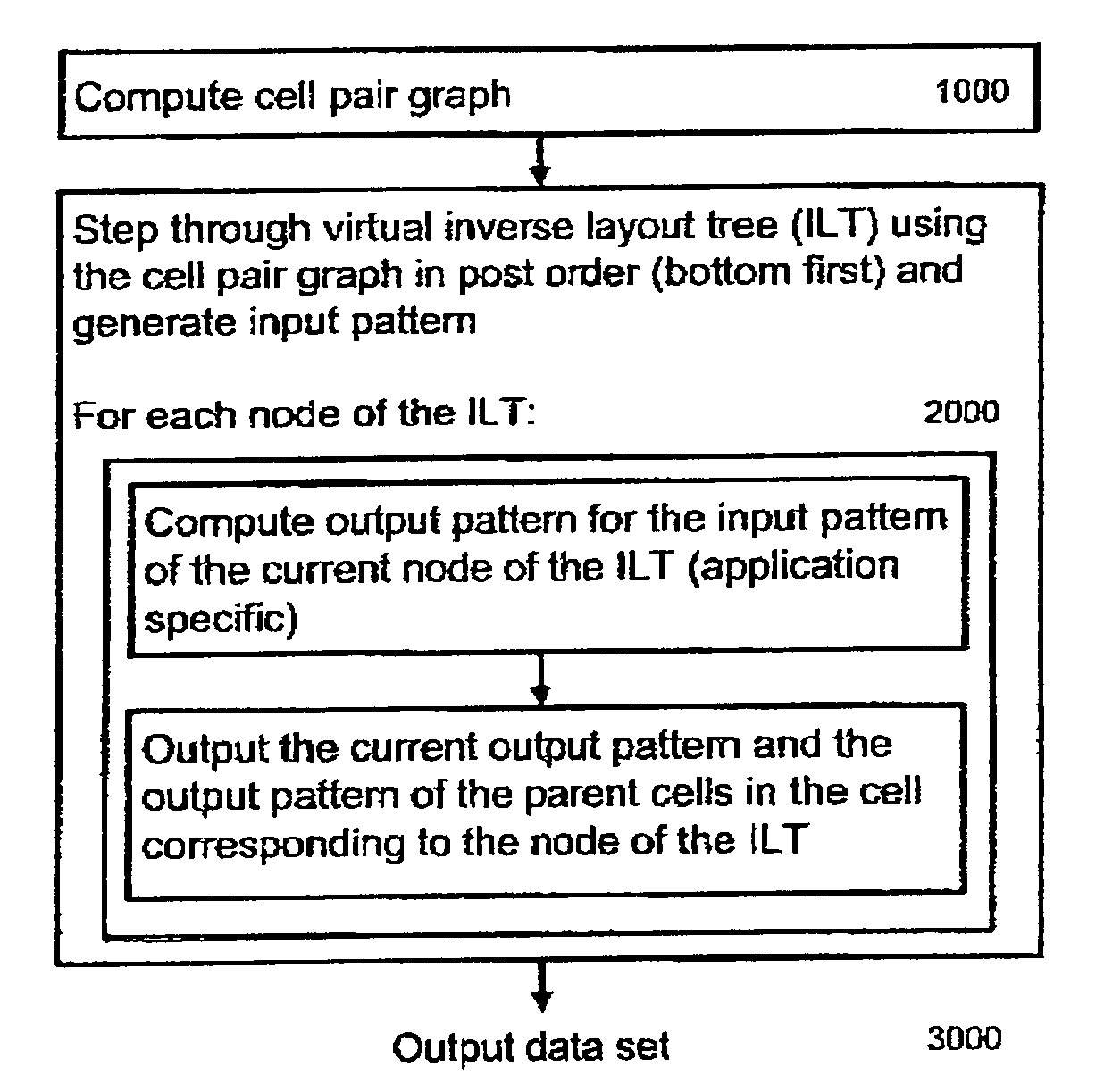
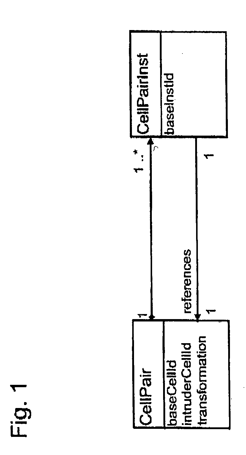
[0038]FIG. 1 shows a cell pair graph with a first node 11 and a second node 12, the arrows 20 forming the edges of the graph.

[0039] Within the design of a layout, the cell pair graph serves to efficiently encode and store interactions between cells of the layout. The data structure used for the cell pair graph herein is produced by determining interacting cells and storing such cells together with hierarchy information.

[0040] Within the scope of the invention, two cells forming a cell pair are considered interacting if an interaction occurs between shapes of the cells or subcells of the cells.

[0041] The first node 11 of a cell pair graph according to FIG. 1 forms a data set called “CellPair” which denotes a cell pair of interacting cells and contains a field for an identifier of a base cell called “baseCellId” and a field for an identifier of an intruding cell (also referred to as intruder cell) called “intruderCellId”. Furthermore, the node CellPair contains a field “transform” ...


PUM


Abstract

At least one cell pair graph is generated for cells of the layout. A partial inverse layout tree is determined from the cell pair graph. For the partial inverse layout tree, only branches of the complete inverse layout tree are considered that describe an interaction between shapes of different cells. A data set is generated from the partial inverse layout tree and the data set is saved, for example, by using the partial inverse layout tree.

Description

[0001] This application claims priority to German Patent Application 10 2005 026 935.4-53 which was filed Jun. 6, 2005 and is incorporated herein by reference. TECHNICAL FIELD [0002] The present invention relates generally to semiconductor devices, and in a particular embodiment to a method and system for performing local geometrical operation on a hierarchical layout of a semiconductor device. BACKGROUND [0003] For the design of an integrated circuit or a structure in semiconductor technology (generally termed “layout”) the verification of each element within a layout against design rules is of great importance. The design rules define the conditions that are, for example, necessary for a successful manufacturing of semiconductor devices. Basic definitions of the terms used in the following description are, for example, found in U.S. Pat. No. 5,528,508, which is incorporated herein by reference. [0004] In the layout of integrated circuits or the layout of other structures of semico...

Claims


Application Information

Patent Timeline
IPC IPC(8): G06F17/50
CPCG06F17/5081G06F30/398
Inventor SEIDL, ALEXANDERMEYER, DIRK
Owner INFINEON TECH AG
Why Eureka
Try Eureka