

Method of forming metal plate pattern and circuit board
- Summary
- Abstract
- Description
- Claims
- Application Information
AI Technical Summary
Benefits of technology
Problems solved by technology
Method used
Image

Examples
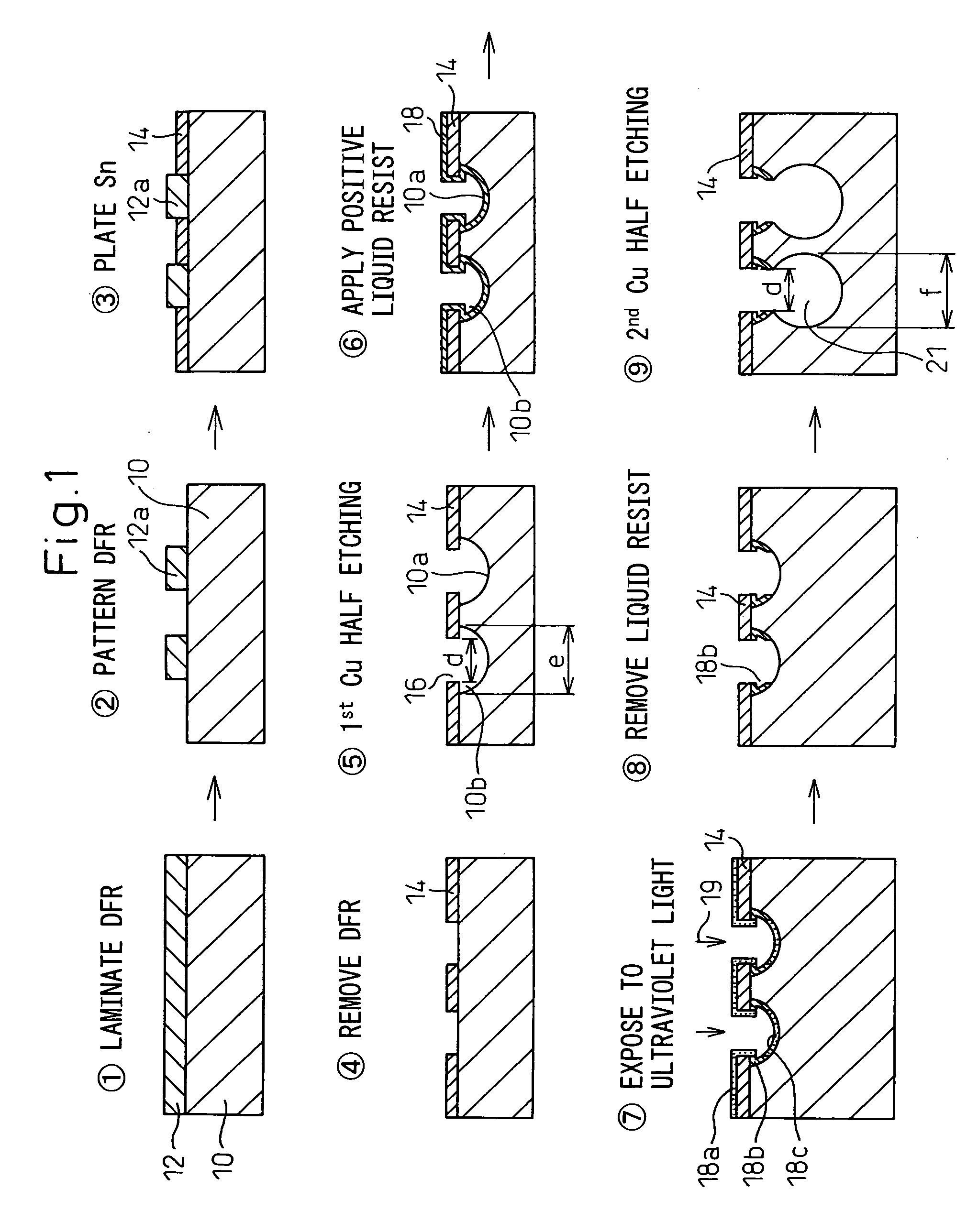
first embodiment
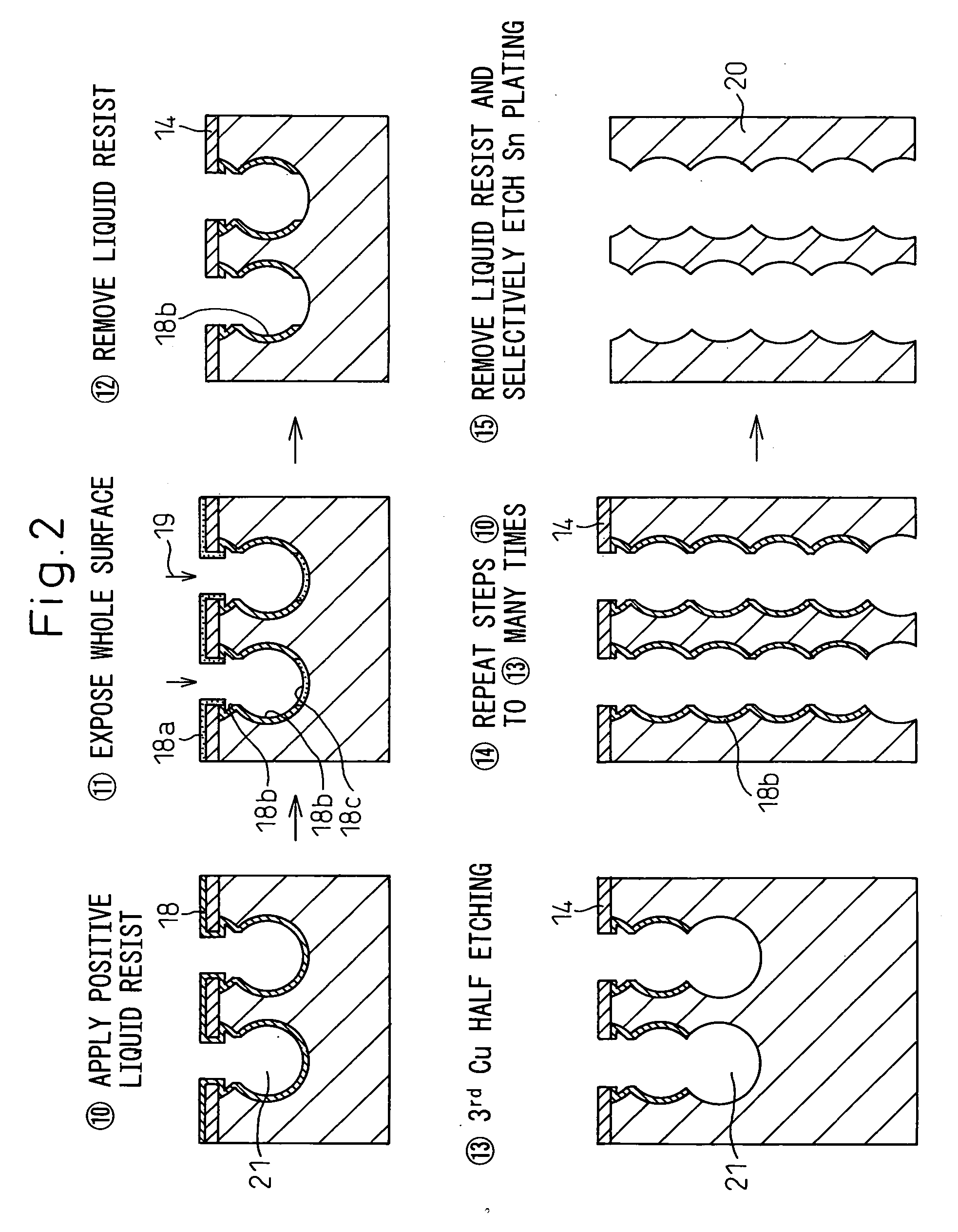
[0044] Next, tenth and subsequent steps are explained with reference to FIG. 2. First, in the tenth step, the positive liquid resist 18 is coated again over the whole surface including the portion subjected to the second half etching in the preceding step.
[0045] In an 11th step, the parallel ultraviolet light 19 is radiated from the upper surface of the positive liquid resist 18 for exposure, followed by development. Like in the seventh step described above, the ultraviolet light used for exposure is desirably the parallel light radiated in the direction perpendicular to the surface of the masking on the metal plate 10. In the case, however, if the light rays can reach deep into the positive liquid resist 18, the ultraviolet light is not necessarily parallel light.
[0046] In this exposure step, the portions of the positive liquid resist 18 exposed to light, i.e. the portion 18a on the tin plating pattern layer 14 of the positive liquid resist 18, the side surface portion of the tin...
second embodiment
[0058] As a result, a high aspect ratio lead or metal pattern 20 a can be finally obtained. Also, the multi-stage etching is carried out from the two surfaces of the metal plate 10, and therefore a metal pattern still higher in aspect ratio can be formed. Further, the multi-stage etching carried out from the two surfaces of the metal plate can form a metal pattern within a shorter length of time.
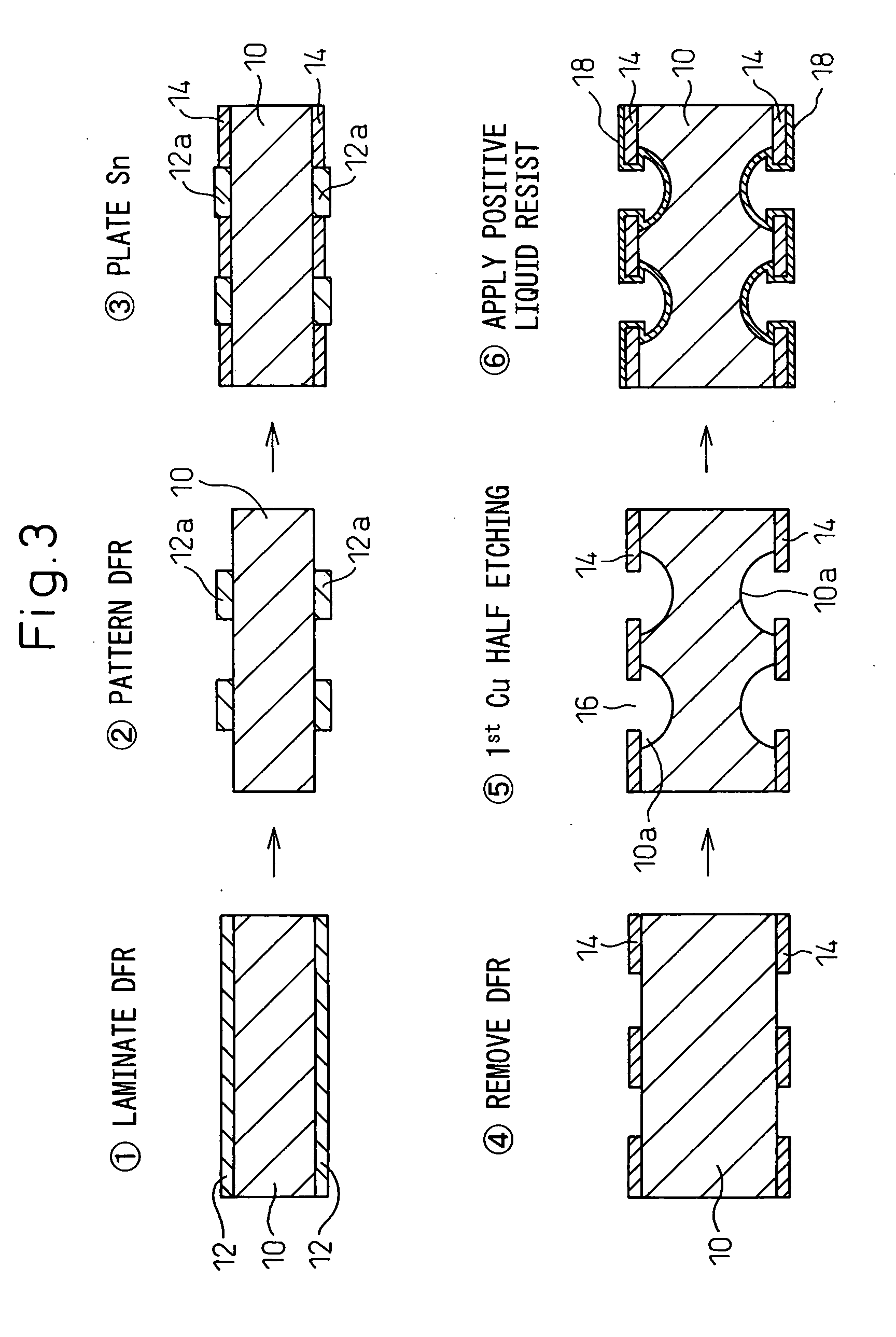
[0059]FIGS. 6 and 7 show the steps of a method of forming a wiring pattern on a circuit board according to a third embodiment of the present invention. In the third embodiment, the circuit board is formed by multi-stage etching, from one surface of the two-side copper-clad resin plate, in which the wiring pattern is formed similarly to the metal plate pattern in the first embodiment.
[0060] In a first step, the whole of one surface of the two-side copper-clad resin plate 30 carrying a copper foil 32 on both surfaces of an insulating base member 31 is coated with a laminate dry film resist (...
fourth embodiment
[0070] FIGS. 8 to 10 show a method, step by step, of forming a conductor pattern on a circuit board according to the present invention.
[0071] According to the fourth embodiment, the circuit board is formed by multi-stage etching from the two surfaces of a two-sided copper-clad resin plate. This embodiment is similar to the third embodiment for forming a circuit board and also similar to the second embodiment in starting the processing from the two surfaces at the same time. Therefore, this embodiment is not described in detail.
[0072] According to the fourth embodiment, a circuit board having a high aspect ratio wiring pattern can be finally formed. The fourth embodiment is explained above with reference to a case having the same wiring pattern on the upper and lower surfaces of the resin substrate 31. Nevertheless, different wiring patterns may be formed concurrently on the upper and lower surfaces of the resin substrate 31 depending on the type of the circuit board.
[0073] In form...
PUM
| Property | Measurement | Unit |
|---|---|---|
| Aspect ratio | aaaaa | aaaaa |
Abstract
Description
Claims
Application Information