Semiconductor device and a method for production thereof

a technology of semiconductor devices and semiconductors, applied in semiconductor devices, basic electric elements, electric devices, etc., can solve the problems of lowering the breakdown voltage of devices, increasing leakage current, and not being suitable for devices of this typ

Active Publication Date: 2007-01-25
CREE SWEDEN
View PDF9 Cites 11 Cited by
  • Summary
  • Abstract
  • Description
  • Claims
  • Application Information

AI Technical Summary

Benefits of technology

[0015] According to another embodiment of the invention the innermost ring of a semiconductor material is laterally spaced with respect to the lateral border of said second layer. This means that there will be a voltage drop between the lateral border of said second layer and this innermost semiconductor material ring reducing electric filed crowding at said lateral border.
[0016] According to another embodiment of the invention said second layer is formed by a metal having a Schottky-barrier with respect to

Problems solved by technology

However, this type of extension means requires an accurately controlled doping of the rings, since the electric field will otherwise be too high at the transitions between adjacent rings reducing the breakdown voltage of the device.
A problem of this solution is that electric field concentrations may result lowering the breakdown voltage o

Method used


Image

  • Semiconductor device and a method for production thereof
  • Semiconductor device and a method for production thereof
  • Semiconductor device and a method for production thereof

Examples


Embodiment Construction

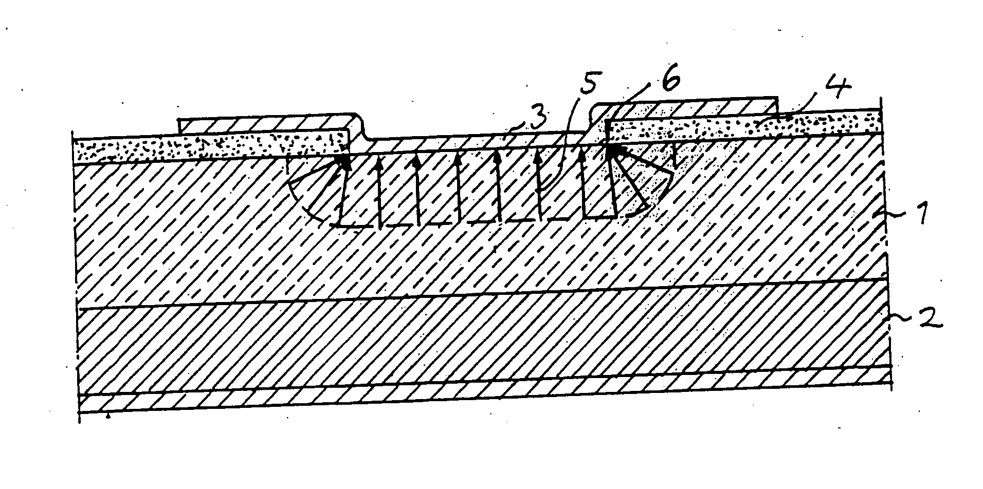
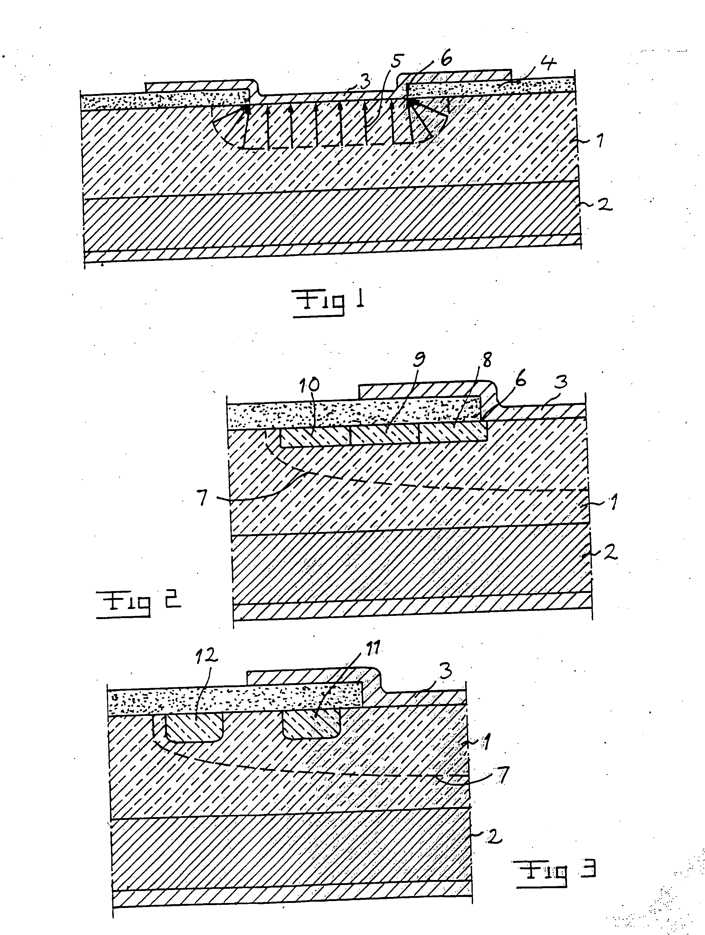
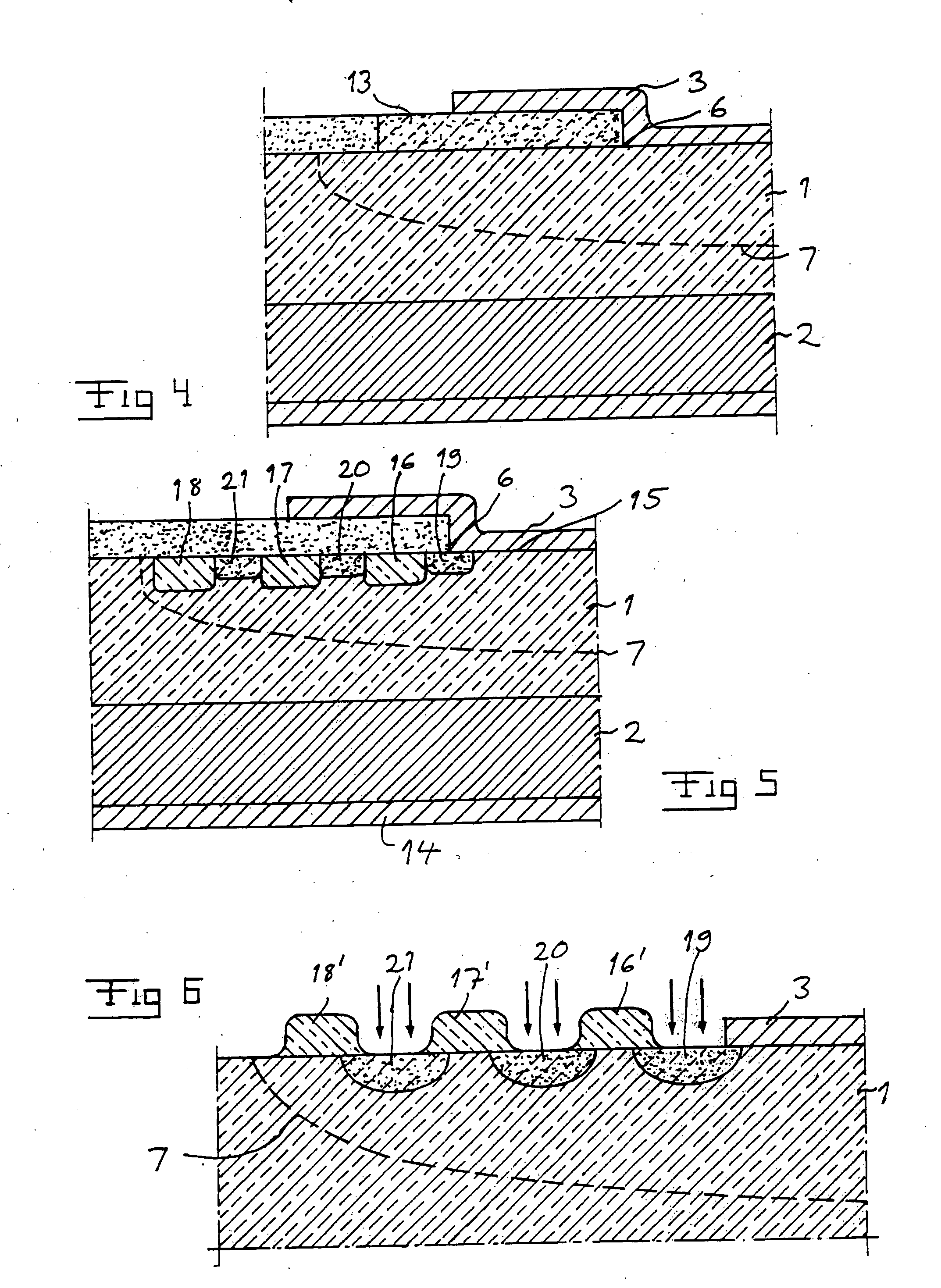
[0036]FIG. 5 illustrates by way of a non-limitative example of a device to which the invention may be applied, a Schottky-diode with two semiconductor layers of SiC, namely a highly doped substrate layer 2 of n-type and a first lightly doped drift layer 1 of n-type. The donors used are for example N or P. The device has also an ohmic metal contact 14 arranged next to the substrate layer and a second layer 3 applied on top of the first layer 1 in the active region of the device, which second layer is formed by a metal having a Schottky-barrier with respect to the semiconductor material of the first layer, i.e. here SiC, for forming a Schottky-junction at the interface between the first layer 1 and the second layer 3. Typical Schottky metals useful for said second layer are Ti, Cr, Al, W, Mo, Ni, Au and Pt.

[0037] A Schottky-diode is provided with an extension means for extending a termination of said Schottky-junction and thereby distributing the electric field within said first laye...


PUM


Abstract

A semiconductor device comprises a first layer (1) of a wide band gap semiconductor material doped according to a first conductivity type and a second layer (3) on top thereof designed to form a junction blocking current in the reverse biased state of the device at the interface to said first layer. The device comprises extension means for extending a termination of the junction laterally with respect to the lateral border (6) of the second layer. This extension means comprises a plurality of rings (16-21) in juxtaposition laterally surrounding said junction (15) and being arranged as seen in the lateral direction away from said junction alternatively a ring (16-18) of a semiconductor material of a second conductivity type opposite to that of said first layer and a ring (19-21) of a semi-insulating material.

Description

TECHNICAL FIELD OF THE INVENTION AND PRIOR ART [0001] The present invention relates to a semiconductor device comprising a first layer of a semiconductor material having an energy gap between the conduction band and the valence band exceeding 2.2 eV and being doped according to a first conductivity type, n or p, and a second layer on top thereof designed to form a junction blocking current in the reverse biased state of the device at the interface to said first layer, said device further comprising extension means for extending a termination of said junction and by that distributing the electric field within said first layer laterally with respect to the lateral border of said second layer. [0002] Thus, the invention is directed to materials having a wide energy gap between the conduction band and the valence band, such as SiC, group 3 B-nitrides and diamond. These materials have in common that they have a higher breakdown field than for instance Si, and this is in the case of SiC m...

Claims


Application Information

Patent Timeline
IPC IPC(8): H01L29/15
CPCH01L29/0619H01L29/872H01L29/66143H01L29/1608
Inventor HARRIS, CHRISTOPHERBASCERI, CEM
Owner CREE SWEDEN
Why Eureka
Try Eureka