Initial-on SCR device for on-chip ESD protection

a technology of esd protection and scr, which is applied in the direction of semiconductor devices, semiconductor/solid-state device details, circuit arrangements, etc., can solve the problems of esd damage becoming the main reliability issue, esd protection design may no longer be able to effectively protect the core circuit against an esd event, and damage to the ic during installation of the i

Active Publication Date: 2007-01-25
IND TECH RES INST
View PDF19 Cites 60 Cited by
  • Summary
  • Abstract
  • Description
  • Claims
  • Application Information

AI Technical Summary

Benefits of technology

[0014] Still in accordance with the present invention, there is provided a method of providing electrostatic discharge (ESD) protection that comprises providing a silicon controlled rectifier (SCR) including a semiconductor substrate and a well formed in the substrate, providing a p-type metal-oxide-semiconductor (PMOS) transistor formed in the well of the SCR including a gate, a first diffused region and a second diffused region spaced apart from the first diffused region, providing an n-type region formed in the well being electrically connected to the first diffused region of the PMOS transistor, providing a p-type region formed in the substrate being electrically connected to the second diffused region of the PMOS transistor, and keeping the PMOS transistor at an on state before an ESD event occurs.
[0015] Yet still in accordance with the present invention, there is provided a method of providing electrostatic discharge (ESD) protection that comprises providing a si

Problems solved by technology

These electrostatic discharges may destroy the IC's during installation of the IC's into products.
ESD damage has become the main reliability issue for complementary metal-oxide-semiconductor (“CMOS”) integrated circuit (“IC”) products fabricated in nanoscale CMOS processes.
However, since the core circuits of the IC fabricated in nanoscale CMOS technology have relatively thin gate oxides, the initial-off ESD protection design may no longer be able to effectively prot

Method used


Image

  • Initial-on SCR device for on-chip ESD protection
  • Initial-on SCR device for on-chip ESD protection
  • Initial-on SCR device for on-chip ESD protection

Examples


Embodiment Construction

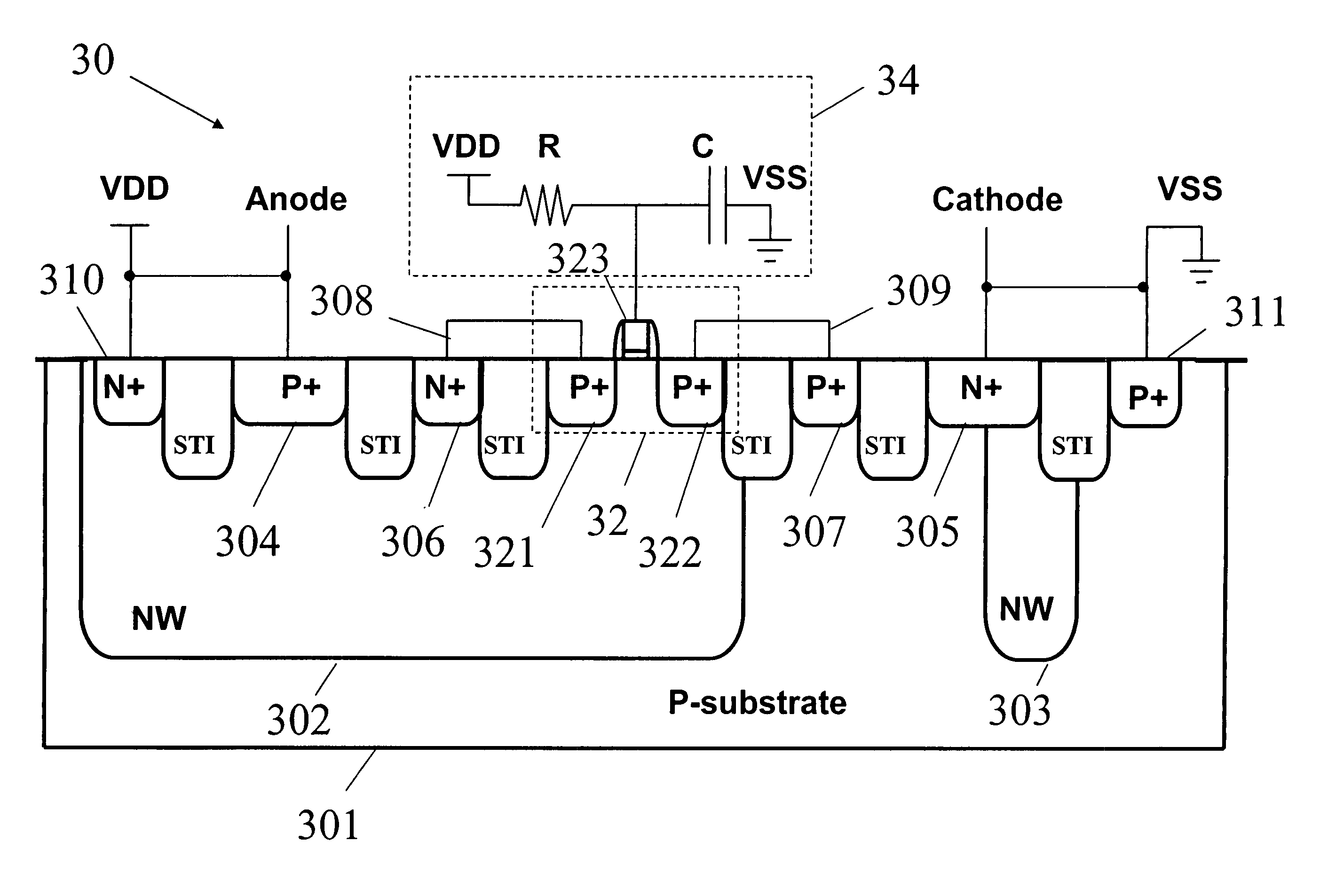
[0036] The present invention provides an initial-on silicon controlled rectifier (“SCR”) that has a relatively low trigger voltage and a relatively fast turn-on speed for on-chip electrostatic discharge (“ESD”) protection. Furthermore, the initial-on SCR device has a holding voltage high enough to prevent latch-up. The initial-on SCR device may be implemented by PMOS-triggered technique without modifying general CMOS processes. For example, the initial-on SCR can be realized in a 0.25-μm CMOS process.

[0037]FIG. 3A is a cross-sectional view of an SCR device 30 in accordance with one embodiment of the present invention. Referring to FIG. 3A, a PMOS transistor 32 is embedded in SCR device 30 to assume an initial-on function together with an ESD detection circuit 34 for ESD protection. SCR device 30 includes a p-type substrate 301, a first n-type well (N-well) region 302 formed in substrate 301, a heavily doped p-type (P+) region 304 formed in N-well 302 to serve as an anode, and a hea...


PUM


Abstract

A semiconductor device for electrostatic discharge (ESD) protection comprises a silicon controlled rectifier (SCR) including a semiconductor substrate, a first well formed in the substrate, a second well formed in the substrate, a first p-type region formed in the first well to serve as an anode, and a first n-type region partially formed in the second well to serve as a cathode, a p-type metal-oxide-semiconductor (PMOS) transistor formed in the first well including a gate, a first diffused region and a second diffused region separated apart from the first diffused region, a second n-type region formed in the first well electrically connected to the first diffused region of the PMOS transistor, and a second p-type region formed in the substrate electrically connected to the second diffused region of the PMOS transistor.

Description

BACKGROUND OF THE INVENTION [0001] 1. Technical Field of the Invention [0002] The present invention relates generally to electrostatic discharge (“ESD”) protection, and more particularly, to a silicon controlled rectifier (“SCR”) device for on-chip ESD protection. [0003] 2. Description of the Related Art [0004] Integrated circuits (IC's) and other semiconductor devices are extremely sensitive to high voltages that may be generated by contact with an electrostatic discharge (“ESD”) event. As such, ESD protection devices are essential for integrated circuits. An ESD event generally results from the discharge of a high voltage potential of several kilovolts, and leads to pulses of high current of several amperes in a short duration of several tens of nanoseconds. An ESD event is generated within an IC by human contact with the leads of the IC or by electrically charged machinery being discharged in other leads of an IC. These electrostatic discharges may destroy the IC's during install...

Claims


Application Information

Patent Timeline
IPC IPC(8): H01L29/417
CPCH01L27/0262H01L23/62H01L2924/0002H01L2924/00
Inventor KER, MING-DOUCHEN, SHIH-HUNGLIN, KUN-HSIEN
Owner IND TECH RES INST
Why Eureka
Try Eureka