Strain inducing multi-layer cap

Inactive Publication Date: 2007-01-25
IQE
View PDF4 Cites 32 Cited by
  • Summary
  • Abstract
  • Description
  • Claims
  • Application Information

AI Technical Summary

Benefits of technology

[0007] Another object of the invention is to provide new and improved strained t

Problems solved by technology

In the semiconductor industry it has recently been discovered that some strain in switching transistors, such as FETs and the like, can actually increase the speed of the transistor.
Similarly, a tensile strain on the channel or active layer of a silicon transistor reduces the number of availa

Method used


Image

  • Strain inducing multi-layer cap
  • Strain inducing multi-layer cap
  • Strain inducing multi-layer cap

Examples


Example

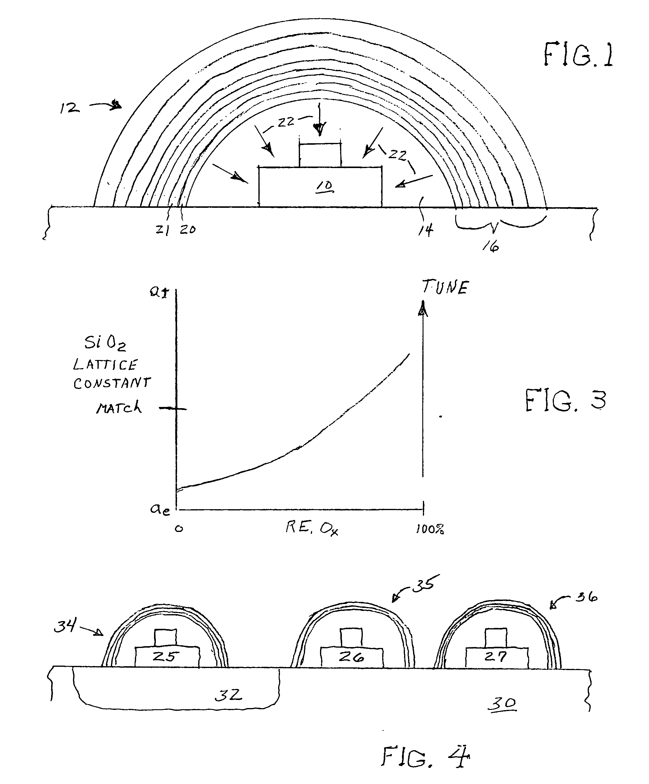
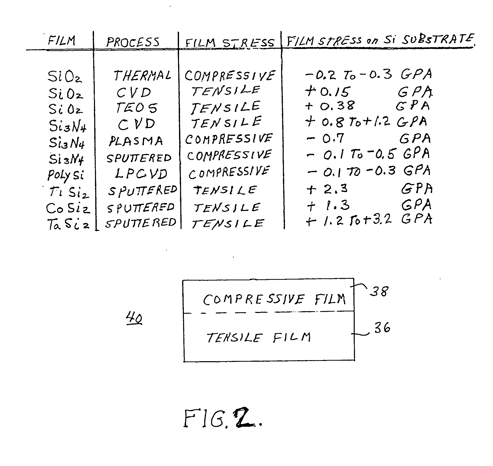
[0016] Turning now to the drawings, attention is first directed to FIG. 1, which illustrates a simplified side view of a transistor 10 with a strain inducing cap 12 thereover. Transistor 10 has an encapsulation or passivation layer 14 deposited thereover in any convenient method. For example, encapsulation layer 14 could be formed of silicon oxide, silicon nitride, or silicon oxynitride or any combination thereof, hereinafter referred to as a ‘silicon insulator’ or ‘silicon insulating material’. Also, encapsulation layer 14 is illustrated as hemispherical or dome shaped for ease of understanding of this description but it will be understood that other shapes might be utilized, depending largely upon the shape of the transistor being strained, the amount and type of strain being induced and any connecting components included. It will be understood that the shape is generally such that at least a portion of the induced strain will be directed along the channel or active layer of trans...


PUM


Abstract

A strained transistor includes a silicon transistor, an encapsulating layer of silicon insulating material with an outer surface, and a stress inducing multilayer cap deposited on the outer surface of the encapsulating layer with at least two layers including a layer of rare earth oxide and a layer including silicon. The stress inducing cap can be designed to provide either compressive strain or tensile strain and virtually any desired amount of strain without producing dislocations, defects, and fractures in the structure.

Description

FIELD OF THE INVENTION [0001] This invention relates to transistors and more specifically to strained transistors. BACKGROUND OF THE INVENTION [0002] In the semiconductor industry it has recently been discovered that some strain in switching transistors, such as FETs and the like, can actually increase the speed of the transistor. For example it has been found that compressive strain on the channel or active layer of a silicon transistor (i.e. a transistor formed on a silicon substrate), e. g. an MOS transistor, increases the number of available electrons and reduces the number of available holes, which increases the speed. Similarly, a tensile strain on the channel or active layer of a silicon transistor reduces the number of available electrons and increases the number of available holes, which reduces the speed. [0003] In one attempt to increase the speed of transistors, an encapsulation or passivation layer is deposited over the transistor. Germanium is then implanted in the enc...

Claims


Application Information

Patent Timeline
IPC IPC(8): H01L27/20
CPCH01L21/768H01L29/7843H01L21/823807H01L21/76832
Inventor ATANACKOVIC, PETAR B.LEBBY, MICHAEL
Owner IQE
Why Eureka
Try Eureka