Method for manufacturing bottom substrate of liquid crystal display device

a liquid crystal display device and substrate technology, applied in the direction of optics, electrical appliances, instruments, etc., can solve the problems of many problems generated by the manufacturing process, the method is not used or approved in the mass-production of tft liquid crystal display devices, and the cost of the apparatus for manufacturing tfd-lcd devices is relatively low, so as to achieve effective increase the yield

Active Publication Date: 2007-01-25
AU OPTRONICS CORP
View PDF0 Cites 18 Cited by
  • Summary
  • Abstract
  • Description
  • Claims
  • Application Information

AI Technical Summary

Benefits of technology

[0009] A method for manufacturing the LCD device substrate is disclosed. The method is achieved by using one photomask including photolithography and etching processes to complete the manufacturing of the LCD device substrate. Through the method, the yield can be effectively increased.

Problems solved by technology

On the other hand, even though manufacturing methods comprising less than four photomasks are suggested, those methods are not used or approved in the mass-production of TFT liquid crystal display devices.
Moreover, the cost for the apparatus for manufacturing a TFD-LCD device is relatively low.
Many problems for the manufacturing-process generate as the size of the manufactured LCD device increases.
For example, the yield of manufacturing is low for large-sized panels.

Method used


Image

  • Method for manufacturing bottom substrate of liquid crystal display device
  • Method for manufacturing bottom substrate of liquid crystal display device
  • Method for manufacturing bottom substrate of liquid crystal display device

Examples


Embodiment Construction

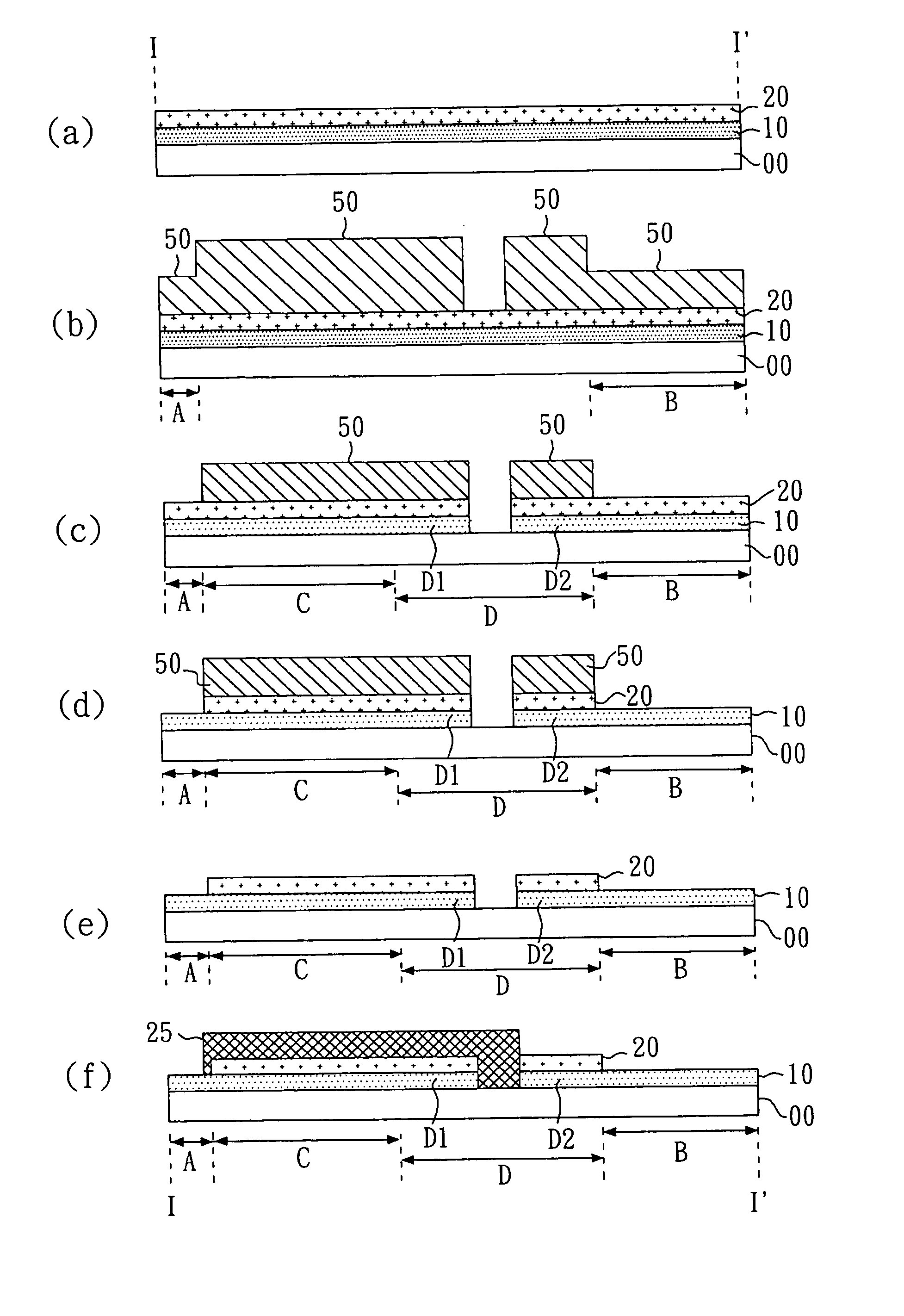
[0018] The patterning process of the method of the present invention is a combination of techniques of partial exposure, etching, and anode oxidation. Through the combination illustrated above, a bottom substrate of a liquid crystal display device can be made through one photomask. The partial exposure of the present invention is preferably performed through halftone masks. The halftone mask includes transparent areas, half-transparent areas, and non-transparent areas. The non-transparent areas are corresponding to the thick photoresist areas on the substrate in future. The half-transparent areas are corresponding to the thin photoresist areas or the cavity areas on the substrate in future.

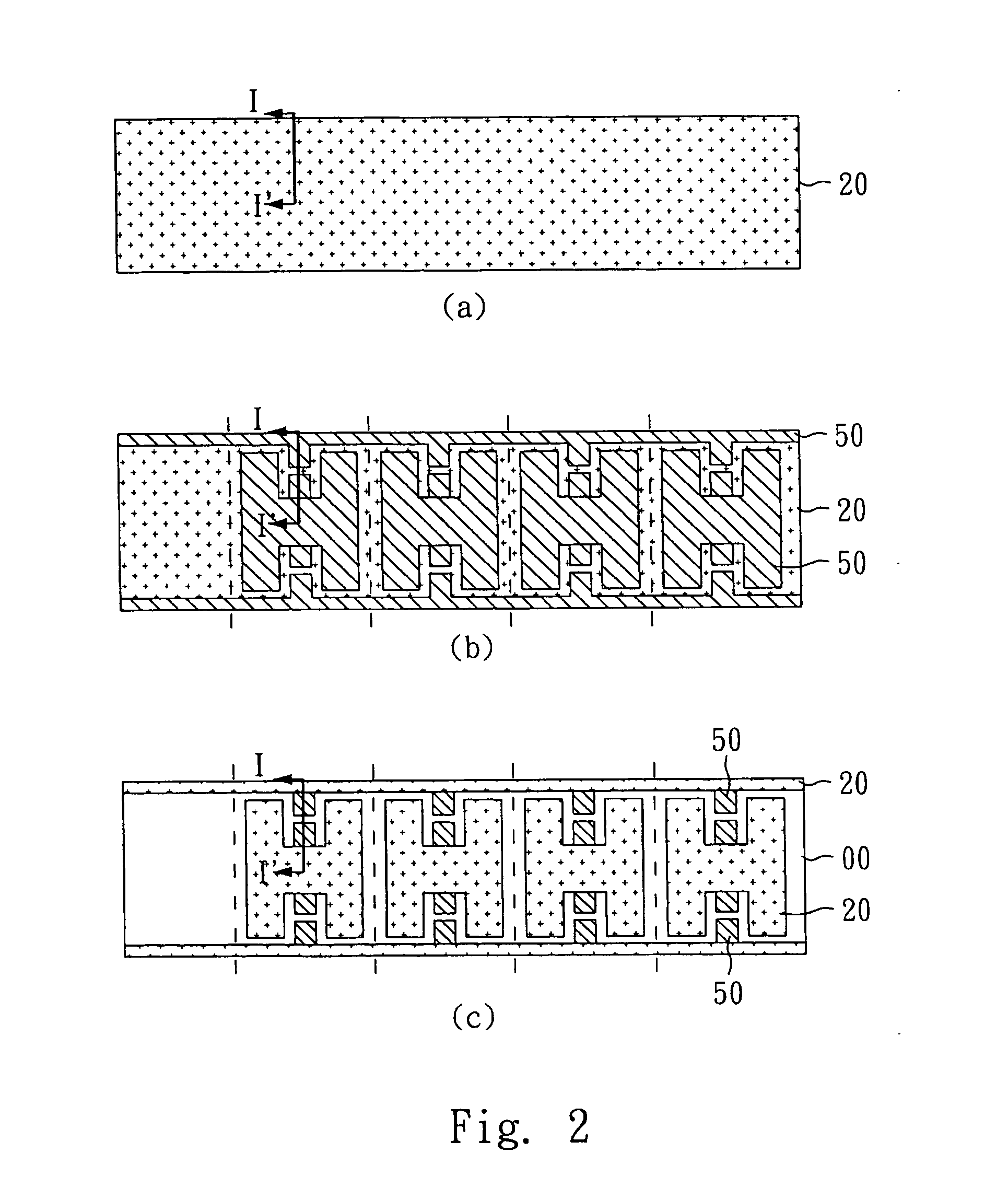
[0019] The FIG. 2 (a) to FIG. 2 (f) are the top views of the patterns of the steps of the method of the present invention. The FIG. 3 (a) to FIG. 3 (f) are the cross section view of the I-I′ line part marked in FIG. 2. For clearly illustrating the method of the present embodiment, the pattern in ...


PUM

PropertyMeasurementUnit
transparentaaaaaaaaaa
thicknessaaaaaaaaaa
sizeaaaaaaaaaa

Abstract

A method for manufacturing liquid crystal display substrates comprises the steps of: (a) providing a substrate having a transparent electrode layer and a metal layer; (b) forming a patterned photoresist layer through half-tone or diffraction; (c) defining signal line area and thin film diode area, or pixel area and conductive electrode-lines by etching; and (d) forming an oxidized layer on partial surface of the metal layer. The disclosure here provides a patterning process of lithography and etching with one photolithography of one single mask in the manufacturing of liquid crystal display substrates. Furthermore, the method disclosed here can effectively increase the yield of manufacturing, and reduce the cost of manufacturing.

Description

BACKGROUND OF THE INVENTION [0001] 1. Field of the Invention [0002] The present invention relates to a method for manufacturing an LCD device substrate, and, more particularly, to a method for manufacturing a thin film diode substrate of a liquid crystal display device having thin film diode arrays. [0003] 2. Description of Related Art [0004] Currently, the active matrix liquid crystal display (LCD) devices are the main products of the flat panel display devices. In the known method for manufacturing a thin film transistor (TFT) liquid crystal display device, the method including five photomasks (or photolithographical steps) is frequently used. Actually, most of the current TFT liquid crystal display devices are produced by methods including four to six photomasks. On the other hand, even though manufacturing methods comprising less than four photomasks are suggested, those methods are not used or approved in the mass-production of TFT liquid crystal display devices. Furthermore, t...

Claims


Application Information

Patent Timeline
Patent Type & Authority Applications(United States)
IPC IPC(8): H01L21/84H01L21/00
CPCG02F2001/136236G02F1/1362G02F1/136236
Inventor CHOU, WENG-BINGYANG, KO-CHING
Owner AU OPTRONICS CORP
Why Eureka
Try Eureka