

Semiconductor device
- Summary
- Abstract
- Description
- Claims
- Application Information
AI Technical Summary
Benefits of technology
Problems solved by technology
Method used
Image

Examples
first embodiment
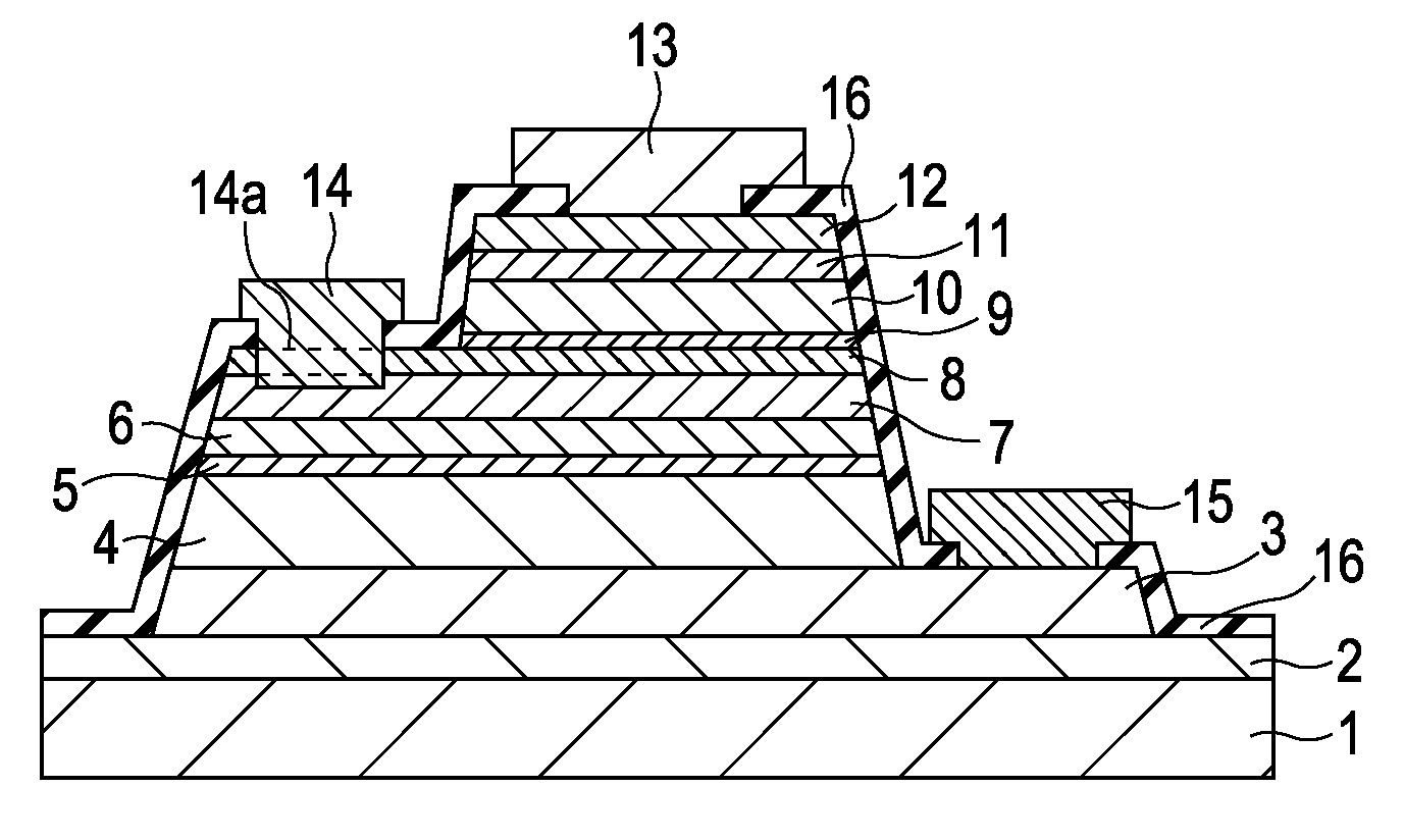
[0073]FIGS. 1 and 2 are each a cross-sectional view of a double-heterojunction HBT according to a first embodiment.
[0074] For example, a buffer layer 2, a subcollector layer 3 composed of n+-type InGaAs, a first collector sublayer 4 (hole-blocking sublayer) composed of n−-type InP, a heavily doped thin sublayer 5 composed of n+-type InP, a graded sublayer 6 composed of n−-type AlInGaAs or the like, a base layer 7 composed of p+-type InGaAs, a graded sublayer 8 composed of n−-type AlInGaAs or the like and having a thickness of about 10 nm, a heavily doped thin sublayer 9 composed of n+-type InP, a first emitter sublayer 10 (hole-blocking sublayer) composed of n−-type InP, a second emitter sublayer 11 composed of n+-type InP, and an emitter cap sublayer 12 composed of n+-type InGaAs are disposed in that order on a semi-insulating semiconductor substrate 1 composed of InP. Furthermore, the surface is covered with an insulating film 16 composed of Si3N4 or the like, except for portions...
second embodiment
[0095]FIG. 15 is a cross-sectional view of a double-heterojunction bipolar transistor according to a second embodiment.
[0096] For example, a subcollector layer 19 composed of n+-type GaAs, a second collector sublayer 20 composed of n−-type GaAs, a first collector sublayer 21 (hole-blocking sublayer) composed of n−-type AlGaAs, a heavily doped thin sublayer 22 composed of n+-type AlGaAs, a graded sublayer 23 composed of n−-type AlGaAs or the like, a base layer 24 composed of p+-type GaAs, a graded sublayer 25 composed of n−-type AlGaAs or the like and having a thickness of about 10 nm, a heavily doped thin sublayer 26 composed of n+-type InGaP, a first emitter sublayer 27 (hole-blocking sublayer) composed of n−-type InGaP, a second emitter sublayer 28 composed of n−-type AlGaAs, a third emitter sublayer 29 composed of n+-type GaAs, and an emitter cap sublayer 30 composed of n+-type InGaAs are laminated in that order on a semi-insulating GaAs semiconductor substrate 17.
[0097] The em...
third embodiment
[0108]FIG. 17 is a cross-sectional view of a double-heterojunction bipolar transistor according to a third embodiment.
[0109] In this embodiment, the double-heterojunction bipolar transistor is disposed on a GaAs substrate, is mainly composed of GaAs, and includes a base layer having electron affinity greater than that of GaAs. For example, a subcollector layer 33 composed of n+-type GaAs, a collector layer 34 composed of n−-type GaAs, a heavily doped thin sublayer 36 composed of n+-type GaAs, a graded sublayer 37 composed of n−-type InGaAs or the like, a base layer 38 composed of p+-type InGaAs, a graded sublayer 39 composed of n−-type AlInGaAs or the like and having a thickness of about 10 nm, a heavily doped thin sublayer 40 composed of n+-type InGaP, a first emitter sublayer 41 composed of n−-type InGaP, a second emitter sublayer 42 composed of n-type GaAs, and an emitter cap sublayer 43 composed of n+-type InGaAs are laminated in that order on a semi-insulating GaAs semiconduct...
PUM
 Abstract
Description
Claims
Application Information