Liquid Crystal Display Device and Driving Method Thereof

a technology of liquid crystal display and driving method, which is applied in the direction of static indicating devices, instruments, etc., can solve the problems of flicker and image sticking to the display image, physical inability to add such test pads, and inability to optimize kickback voltage compensation, so as to minimize the deterioration of picture quality

Inactive Publication Date: 2007-02-01
SAMSUNG ELECTRONICS CO LTD
View PDF0 Cites 97 Cited by
  • Summary
  • Abstract
  • Description
  • Claims
  • Application Information

AI Technical Summary

Benefits of technology

[0014] It is therefore an object of the present invention to provide an LCD device which is capable of minimizing deterioration in picture quality caused by a kickback voltage, and a driving method thereof.

Problems solved by technology

By this kickback voltage, the pixel voltage signal applied to the pixel electrode of the liquid crystal cell varies and thus flicker and image sticking appear on the display image.
However, since the kickback voltage does not have the same value on all the liquid crystal cells arranged in the LCD panel, it is not possible to optimize the kickback voltage compensation.
However, it is physically impossible to add such test pads because there is no design margin in a typical LCD panel.

Method used


Image

  • Liquid Crystal Display Device and Driving Method Thereof
  • Liquid Crystal Display Device and Driving Method Thereof
  • Liquid Crystal Display Device and Driving Method Thereof

Examples


first embodiment

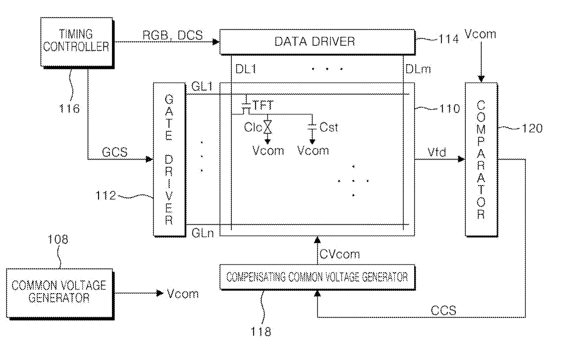
[0051]FIG. 3 is a block diagram of an LCD device according to the present invention.

[0052] Referring to FIG. 3, the LCD device includes an LCD panel 110, a data driver 114 for supplying a pixel voltage signal to data lines DLl to DLm of the LCD panel 110, a gate driver 112 for supplying a scan signal to gate lines GLl to GLn, a timing controller 116 for controlling the data driver 114 and the gate driver 112 by using a synchronization signal received from a system, a comparator 120 for comparing the pixel voltage signal which is fed back from the LCD panel 110 with a common voltage, and a compensating common voltage generator 118 for adjusting the common voltage according to an output result of the comparator 120.

[0053] The timing controller 116 rearranges digital video data RGB received from a graphic controller of the system and supplies the rearranged data to the data driver 114.

[0054] The timing controller 116 generates a gate control signal GCS for controlling the gate driver...

second embodiment

[0075]FIG. 9 is a circuit diagram illustrating an LCD panel of an LCD device according to the present invention.

[0076] Referring to FIG. 9, the LCD panel of the LCD device has the same elements as the LCD panel shown in FIG. 4 except that dummy liquid crystal cells DClc, dummy thin film transistors DTFT and dummy storage capacitors DCst are additionally provided.

[0077] The dummy liquid crystal cells DClc are arranged in a matrix configuration at intersections of a dummy data line DDL and gate lines GLl to GLn. Dummy thin film transistors DTFT connected to the respective dummy liquid crystal cells DClc supply a pixel voltage signal received through the dummy data line DDL to the dummy liquid crystal cells DClc in response to a scan signal received from the gate line.

[0078] Alternatively, the dummy liquid crystal cells DClc are arranged in a matrix configuration at intersections of a dummy gate line DGL and the data lines DLl to DLm, as shown in FIG. 10. Dummy thin film transistors ...

third embodiment

[0081]FIG. 11 is a circuit diagram illustrating a compensating common voltage generator of an LCD device according to the present invention.

[0082] The LCD device shown in FIG. 11 has the same elements as the LCD device shown in FIG. 3 except that a resistor group connected to an output terminal of the compensating common voltage generator, and a selector are added. Therefore, a detailed description of the same elements will be omitted.

[0083] The compensating common voltage generator 118 includes a resistor group 134 connected to an output terminal of the common voltage generator 108 for generating a common voltage and includes a selector 130.

[0084] The resistor group 134 is connected to an output terminal of the common voltage generator 108 and includes a plurality of compensating resistors Rc1 to Rck having different resistances. This resistor group 134 receives the common voltage Vcom generated from the common voltage generator 108 and generates different compensating common vol...


PUM


Abstract

Disclosed is a liquid crystal display (LCD) device which is capable of minimizing deterioration in picture quality caused by a kickback voltage, and a driving method thereof. The LCD device includes an LCD panel having a plurality of liquid crystal cells to which a pixel voltage signal is supplied, and a compensating common voltage generator for generating different compensating common voltages according to a pixel voltage signal which is fed back from the LCD panel.

Description

CROSS-REFERENCE TO RELATED APPLICATION [0001] This application claims priority to Korean Patent Application No. 2005-70199 filed on Aug. 1, 2005, the contents of which are hereby incorporated by reference in their entirety. BACKGROUND OF THE INVENTION [0002] 1. Field of the Invention [0003] The present invention relates to a liquid crystal display (LCD) device and a driving method thereof, and more particularly, to an LCD device that is capable of minimizing deterioration in picture quality caused by a kickback voltage, and a driving method thereof. [0004] 2. Description of the Related Art [0005] A typical LCD device displays images by controlling the light transmittance of a liquid crystal by an electric field. This LCD device includes an LCD panel in which a matrix of liquid crystal cells is arranged, and a driving circuit for driving the LCD panel. [0006] The LCD panel includes, as illustrated in FIG. 1, a gate line GL, a data line DL crossing the gate line GL, and a thin film tr...

Claims


Application Information

Patent Timeline
Patent Type & Authority Applications(United States)
IPC IPC(8): G09G3/36
CPCG09G3/3614G09G3/3648G09G2320/043G09G2320/0247G09G2320/029G09G3/3655G09G3/36
Inventor KIM, MAN SUNGKIM, KYUNG YUL
Owner SAMSUNG ELECTRONICS CO LTD
Why Eureka
Try Eureka