Programmable semiconductor device containing a vertically notched fusible link region and methods of making and using same

a technology of fusible link region and programmable semiconductor, which is applied in the direction of semiconductor devices, semiconductor/solid-state device details, electrical apparatus, etc., can solve the problems of significant amount of real estate consumed by each fuse, significant increase in the delay in response and power consumption of the fuses not only for programming, but also for reading

Inactive Publication Date: 2007-02-08
IBM CORP
View PDF12 Cites 123 Cited by
  • Summary
  • Abstract
  • Description
  • Claims
  • Application Information

AI Technical Summary

Benefits of technology

[0023] Other aspects, features and advantages of the invention will be more fully apparent from the ensuing disclosure and appended claims.

Problems solved by technology

An anti-fuse, on the other hand, is normally open or has relatively high resistance, and when an anti-fuse is blown or programmed, this results in a short circuit or a decreased resistance.
Additionally, due to laser size, depth penetration, and thermal considerations, these fuses must be placed in relative isolation, with no other active circuits adjacent, or in vertical proximity, thus a significant amount of real estate is consumed for each fuse.
), much higher programming currents and longer response time are required in order to generate enough joule heat for melting the high temperature silicide material, which significantly increases the delay in response and the power consumption of the fuses not only for programming, but also for reading.

Method used


Image

  • Programmable semiconductor device containing a vertically notched fusible link region and methods of making and using same
  • Programmable semiconductor device containing a vertically notched fusible link region and methods of making and using same
  • Programmable semiconductor device containing a vertically notched fusible link region and methods of making and using same

Examples


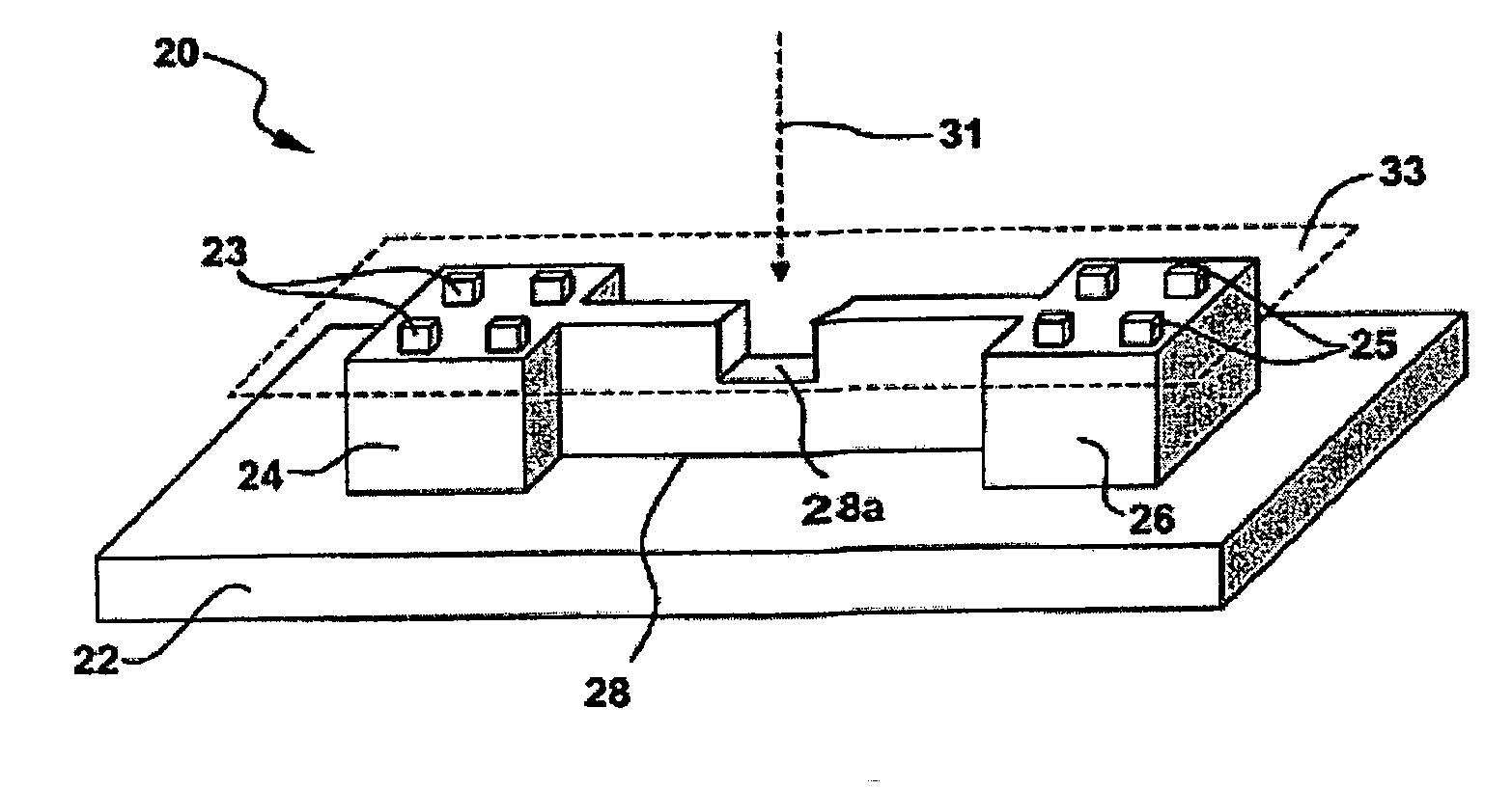
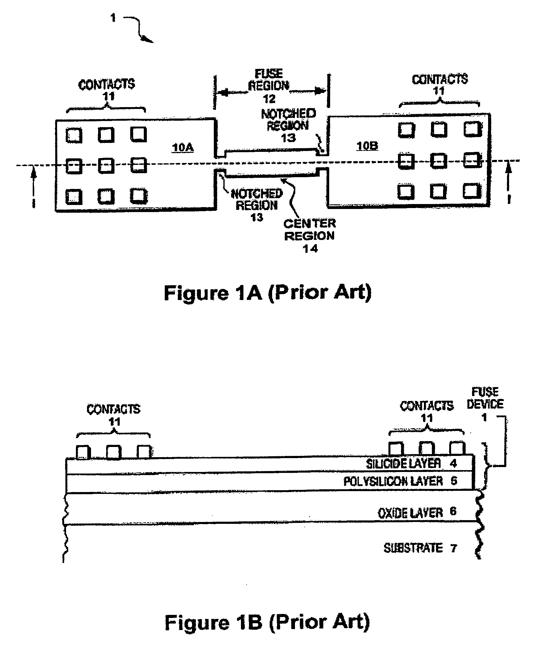
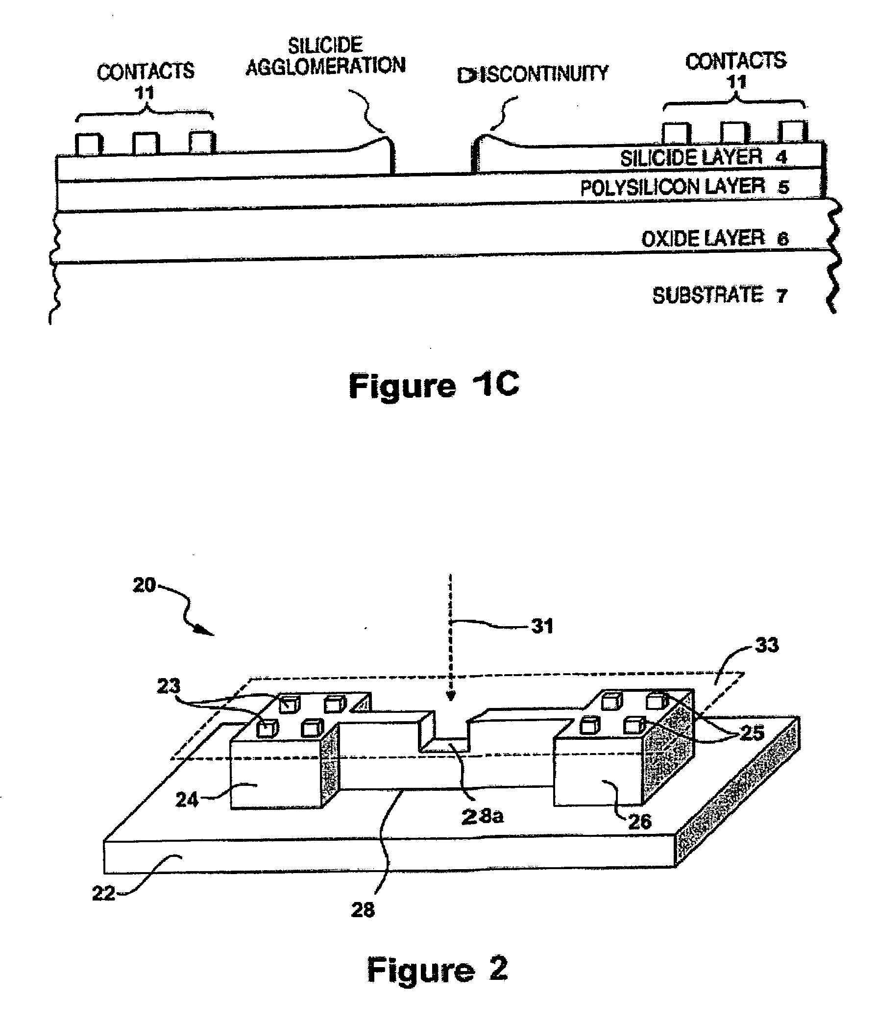
Embodiment Construction

[0036] In the following description, numerous specific details are set forth, such as particular materials, dimensions, numbers of contacts, programming voltages and currents, in order to provide a thorough understanding of the invention. However, it will be appreciated by one of ordinary skill in the art that the invention may be practiced without these specific details. In other instances, well-known structures, and circuits have not been described in detail in order to avoid obscuring the invention.

[0037] It will be understood that when an element as a layer, region or substrate is referred to as being “on” another element, it can be directly one the other element or intervening elements may also be present. In contrast, when an element is referred to as being “directly on” another element, there are no intervening elements present. It will also be understood that when an element is referred to as being “connected” or “coupled” to another element, it can be directly connected or...


PUM


Abstract

The present invention relates to a programmable semiconductor device, preferably a FinFET or tri-gate structure, that contains a first contact element, a second contact element, and at least one fin-shaped fusible link region coupled between the first and second contact elements. The second contact element is laterally spaced apart from the first contact element, and the fin-shaped fusible link region has a vertically notched section. A programming current flowing through the fin-shaped fusible link region causes either significant resistance increase or formation of an electric discontinuity in the vertically notched section. Alternatively, the vertically notched section may contain a dielectric material, and application of a programming voltage between a gate electrode overlaying the vertically notched section and one of the contact elements breaks down the dielectric material and allows current flow between the gate electrode and the fin-shaped fusible link region.

Description

FIELD OF THE INVENTION [0001] The present invention relates generally to programmable semiconductor devices that comprise electrical fuse and / or anti-fuse and methods of making and using such devices. More specifically, the present invention relates to electrical fuse and / or anti-fuse device structures that have a fin-shaped fusible link region with a vertical notch therein. BACKGROUND OF THE INVENTION [0002] Fuses and anti-fuses are programmable electronic devices that are used in a variety of circuit applications. A fuse is normally closed or has a relatively lower resistance to allow electric current flowing therethrough, and when blown or programmed, it becomes open or has an increased resistance. An anti-fuse, on the other hand, is normally open or has relatively high resistance, and when an anti-fuse is blown or programmed, this results in a short circuit or a decreased resistance. [0003] There are many applications for fuses and anti-fuses. One particular application is for c...

Claims


Application Information

Patent Timeline
Patent Type & Authority Applications(United States)
IPC IPC(8): H01L27/10
CPCH01L23/5256H01L27/10H01L29/66795H01L29/785H01L2924/0002H01L2924/00
Inventor NOWAK, EDWARD J.RANKIN, JED H.TONTI, WILLIAM R.
Owner IBM CORP
Why Eureka
Try Eureka