

Semiconductor manufacturing device and its heating unit
- Summary
- Abstract
- Description
- Claims
- Application Information
AI Technical Summary
Benefits of technology
Problems solved by technology
Method used
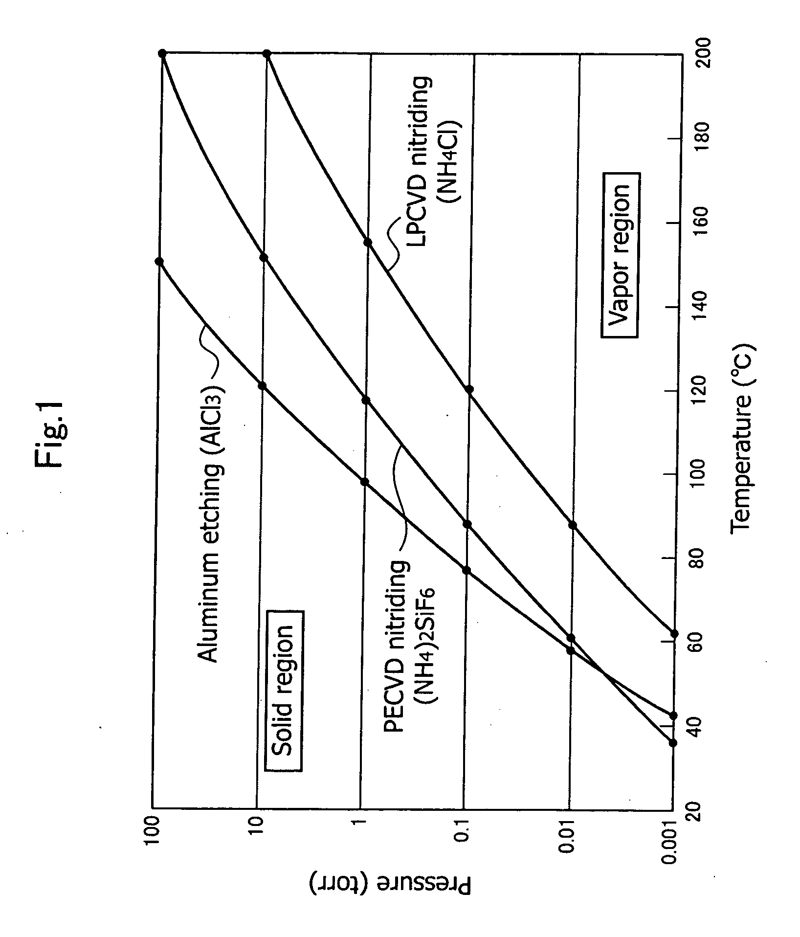
Image

Examples
Embodiment Construction
[0077] Hereinafter, best modes of the present invention are described with reference to the accompanying drawings.
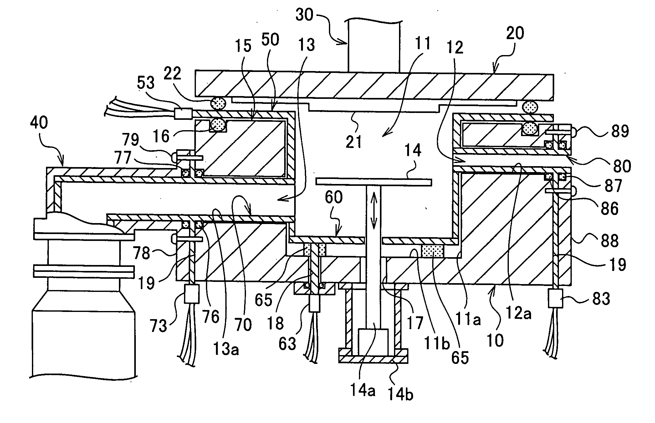
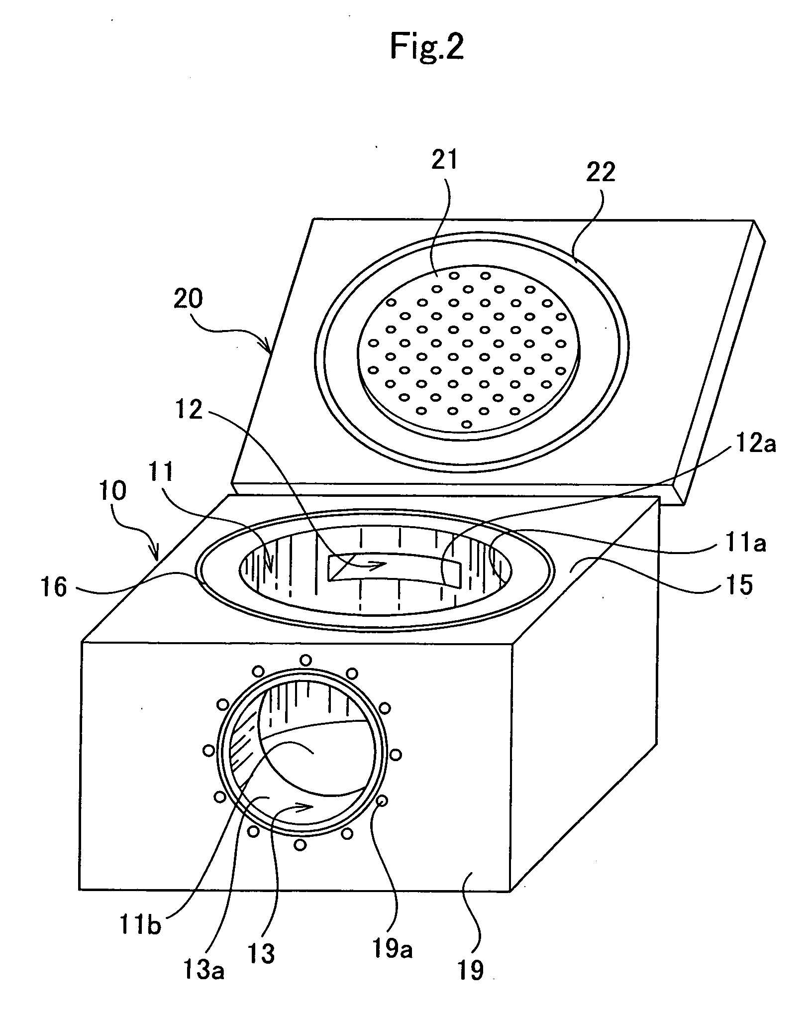
[0078] A semiconductor manufacturing device (CVD device) having the heating unit according to the present invention includes, as shown in FIG. 2 and FIG. 3, a main body 10, a cover 20 connected to the main body 10 so as to open and close the main body 10, a supply line 30 for supplying a processing gas or the like connected to the cover 20, and an exhaust line 40 that is connected to the main body 10 and that includes a turbo molecular pump (TMP) on the downstream side.
[0079] The main body 10 has a processing chamber 11 forming a cylindrical space for housing a semiconductor wafer and applying predetermined processes, a transferring passage 12 with a roughly rectangular section for putting in and taking out wafers of the processing chamber 11, an roughly cylindrical exhaust passage 13 for exhausting a processing gas inside the processing chamber, and a susceptor 14 on ...
PUM
| Property | Measurement | Unit |
|---|---|---|
| Temperature | aaaaa | aaaaa |
| Adhesion strength | aaaaa | aaaaa |
| Efficiency | aaaaa | aaaaa |
Abstract
Description
Claims
Application Information