Semiconductor device and method of generating a reference voltage therefor

a technology of a reference voltage and a semiconductor, applied in the field of semiconductor devices, can solve the problems of deterioration phenomenon, charge falling off, and change amount, and achieve the effect of increasing and decreasing the number of voltage outputs, and being easy to adjus

Inactive Publication Date: 2007-02-15
MONTEREY RES LLC
View PDF2 Cites 13 Cited by
  • Summary
  • Abstract
  • Description
  • Claims
  • Application Information

AI Technical Summary

Benefits of technology

[0013] A more specific object of the present invention is to provide a semiconductor device that can set an optimum reference voltage according to changes with age in the internal reference cells, and a method of generating a reference voltage.
[0014] The above objects of the present invention are achieved by a semiconductor device that includes at least one reference cell, a cascode circuit that has at least two current mirror circuits and outputs voltages dependent on a current flowing through the at least one reference cell to at least two output paths, and a switch that selectively connects the at least two output paths to a given output terminal. With this structure, the number of voltage outputs can be increased and decreased without an increase in the number of reference cells. Accordingly, the reference voltage determined from those voltages can be readily adjusted and reading can be performed without a decrease in margin at the time of data reading from the core cell.
[0015] The above objects of the present invention are also achieved by a semiconductor device that includes at least one internal reference cell that is provided in a core cell array, at least one external reference cell that is provided outside the core cell array, a first cascode circuit that has at least two current mirror circuits and outputs first voltages dependent on a current flowing through the at least one internal reference cell to at least two first output paths; a first switch that selectively connects the at least two first output paths to a given output terminal so that a selected first voltage is applied to the given output terminal, and a second cascode circuit that converts a current flowing through the at least one external reference cell into a second voltage. With this structure, the number of voltage outputs can be increased and decreased, without an increase in the number of internal and external reference cells. An internal reference cell deteriorates due to changes with age. Since the degree of deterioration varies among reference cells, voltages that are read out from the reference cells also vary. As a result, the reference voltage generated from the voltages of the reference cells is not constant. Therefore, the number of voltage outputs is increased and decreased, so as to adjust the reference voltage. Thus, reading can be performed without a decrease in margin at the time of data reading from the core cell.
[0016] In a semiconductor device in accordance with the present invention, the second cascode circuit may have at least two current mirror circuits that generate the second voltages from the current flowing through the at least one external reference cell, with the second voltages being applied to at least two second output paths. Also, the semiconductor device may further include a second switch that selectively connects the at least two second output paths to the given output terminal. Thus, the number of voltage outputs can be increased and decreased, without an increase in the number of external reference cells.
[0018] In this semiconductor device, the at least one internal reference cell may include a first cell having a data state “0” and a second cell having a data state “1”, while the at least one external reference cell has an intermediate state between data states “0” and “1”. Accordingly, the data written in the core cell can be read out with high precision.
[0021] The above objects of the present invention are also achieved by a method of generating a reference voltage that includes the steps of generating voltages from a current flowing through a reference cell, the voltages being applied to at least two output paths and selectively connecting the at least two output paths to a given terminal at which a reference voltage is available. In accordance with this method, the reference voltage determined by the voltages can be readily adjusted and reading can be performed without a decrease in margin at the time of data reading from the core cell.

Problems solved by technology

The core cell, however, deteriorates as data is written and erased.
As a result, a deterioration phenomenon is observed wherein charges fall off with time.
However, the amount of change with age varies among the reference cells, and the problem of a decrease in margin at the time of reading is still present, even with the addition of the external reference cell.

Method used


Image

  • Semiconductor device and method of generating a reference voltage therefor
  • Semiconductor device and method of generating a reference voltage therefor
  • Semiconductor device and method of generating a reference voltage therefor

Examples


Embodiment Construction

[0032] The following is a description of preferred embodiments of the present invention, with reference to the accompanying drawings.

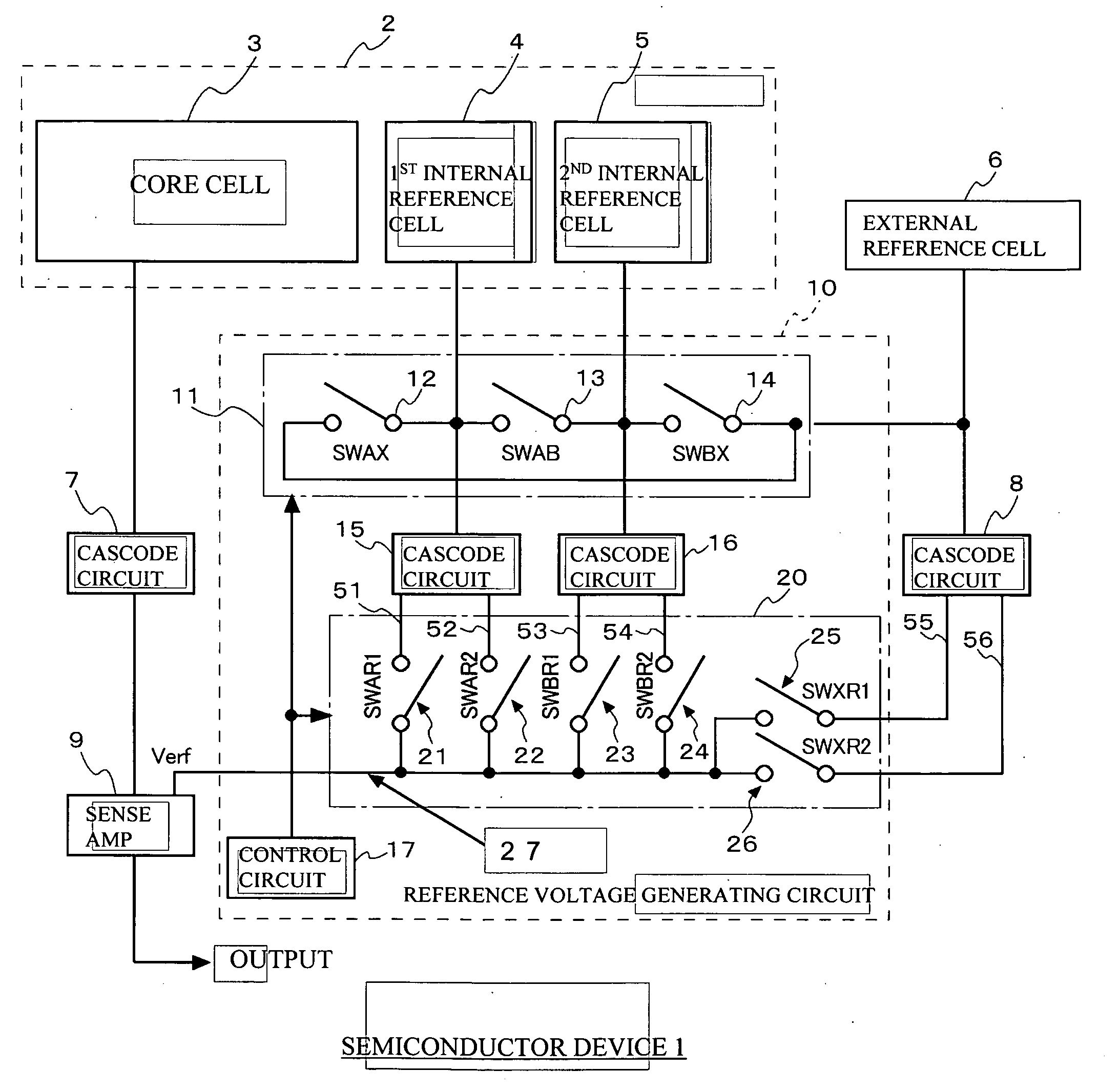
[0033] Referring first to FIG. 4, the structure in accordance with an embodiment of the present invention is described. A semiconductor device 1 in accordance with this embodiment is a non-volatile semiconductor device that has two internal reference cell regions in a core cell array 2 and an external reference cell outside the core cell array 2. The core cell array 2 is a virtual ground memory cell array, containing memory cells, word lines, bit lines, and the like. Two-bit data is stored in each of the memory cells. A film formed by stacking an oxide film, a nitride film, and an oxide film in this order is interposed between a control gate and a substrate. Charges are trapped in the nitride film so as to change the threshold value thereof. By doing so, data “0” and data “1” are distinguished from each other. Since a trap layer such as the nitride fi...


PUM


Abstract

A semiconductor device includes at least one reference cell (6), a cascode circuit (8) that has at least two current mirror circuits (30, 33 and 30, 34) and outputs voltages dependent on a current flowing through the at least one reference cell (6) to at least two output paths (55, 56), and a switch (20) that selectively connects the at least two output paths (55, 56) to a given output terminal (27).

Description

CROSS-REFERENCES TO RELATED APPLICATIONS [0001] This is a continuation of International Application No. PCT / JP2005 / 006266, filed Mar. 31, 2005 which was not published in English under PCT Article 21(2). BACKGROUND OF THE INVENTION [0002] 1. Field of the Invention [0003] The present invention relates to semiconductor devices and, more particularly, to a semiconductor memory device that includes a reference cell to set a reference level for reading and writing independent of memory cells, and uses the reference level during data writing and data read verify. [0004] 2. Description of the Related Art [0005] In a semiconductor device, especially in a non-volatile memory device, reference memory cells for reference at the time of memory cell reading are provided independently of regular memory cells. For instance, a core cell, a first internal reference cell, and a second internal reference cell are provided in a core cell region that stores data. A reference voltage is generated based on...

Claims


Application Information

Patent Timeline
IPC IPC(8): G11C16/06
CPCG11C16/28G11C7/14
Inventor TSUKIDATE, YOSHIHIRO
Owner MONTEREY RES LLC
Why Eureka
Try Eureka