Semiconductor device using EPI-layer and method of forming the same

Active Publication Date: 2007-02-15
TAIWAN SEMICON MFG CO LTD
View PDF6 Cites 15 Cited by
  • Summary
  • Abstract
  • Description
  • Claims
  • Application Information

AI Technical Summary

Benefits of technology

[0017] As described above, the present invention can reduce or prevent surface damage to a semiconductor substrate, which may occur when of performing an ion implantation for controlling a threshold voltage. Furthermore, one does not need to perform an anneal after ion implanta

Problems solved by technology

However, the ions injected in the ion implantation apparatus are collided with a wafer, which can induce strains and defects.
Namely, peripheral portions of the isolating oxide film may spread to reduce the active areas where circuit e

Method used


Image

  • Semiconductor device using EPI-layer and method of forming the same
  • Semiconductor device using EPI-layer and method of forming the same
  • Semiconductor device using EPI-layer and method of forming the same

Examples


Embodiment Construction

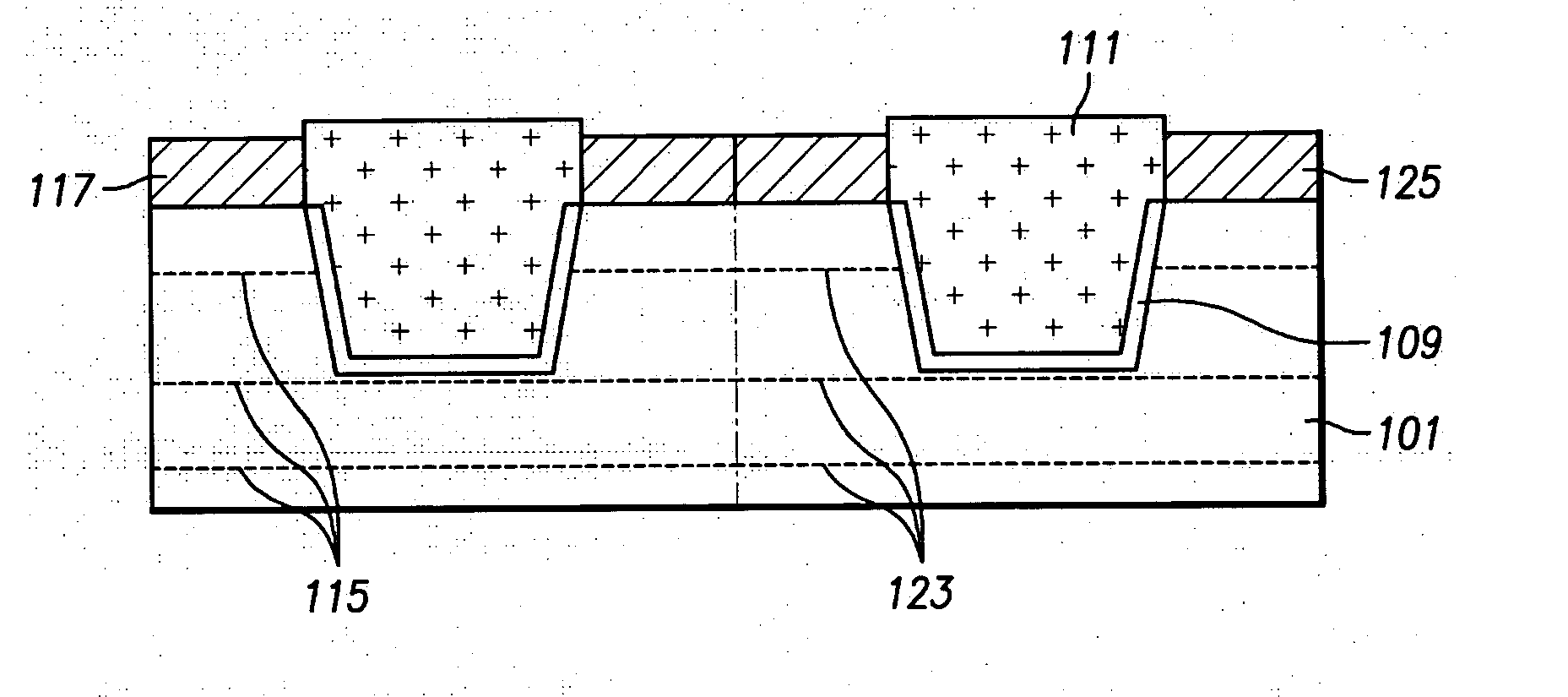
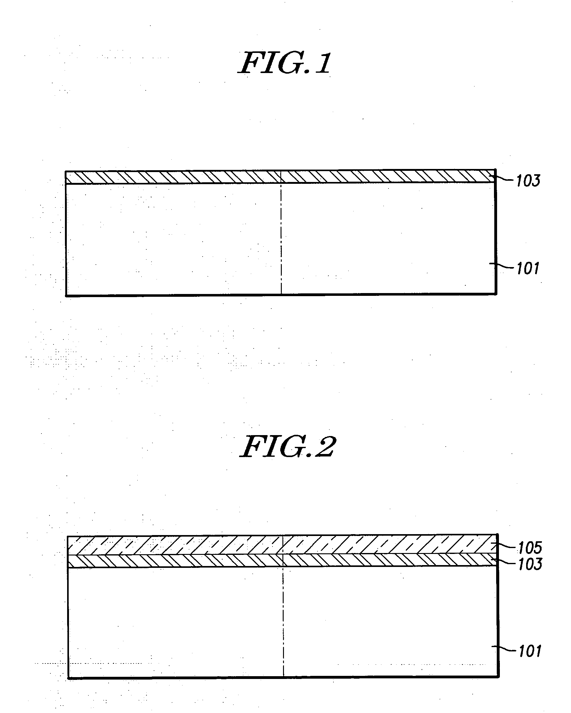
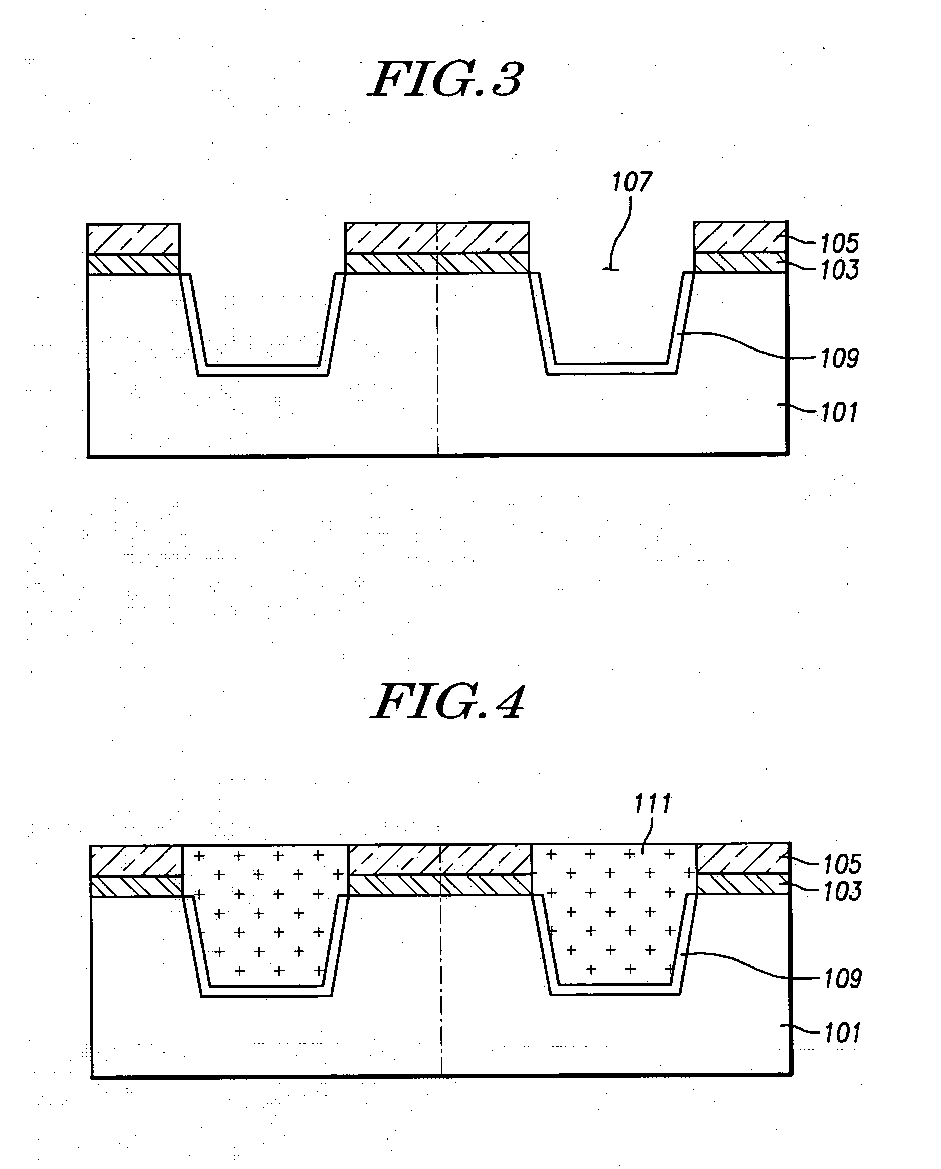
[0020] Hereinafter, a preferred embodiment of the present invention will be described in detail with reference to the accompanying drawings. A shape and thickness of a layer and a member are exaggerated or schematic in the drawings. The same reference numerals are used throughout the drawings to indicate the same elements.

[0021] Referring to FIG. 1, a pad oxide film 103 is formed in a thickness of 50˜150 Å on a semiconductor substrate 101, using an oxygen gas and a hydrogen gas. The pad oxide film 103 mitigates stresses of the semiconductor substrate 101 and a nitride film to be formed hereafter, and protects the semiconductor substrate 101 in an ion implantation process, and further participates in a project region Rp of the ion implantation.

[0022] Referring to FIG. 2, a nitride film 105 is formed in a thickness of 1,000˜3,000 Å on the pad oxide film 103, using NH3 gas and SiH2Cl2 gas at a pressure of 0.2˜0.25 torr. The nitride film 105 is used as an etch or polish stop layer for...


PUM


Abstract

A method of fabricating a semiconductor device includes forming a pad oxide film and a nitride film on a semiconductor substrate; exposing the semiconductor substrate by selectively etching the pad oxide film and the nitride film; forming a trench in the exposed semiconductor substrate; forming a gap-fill dielectric film in the trench; exposing an active area of the semiconductor substrate by removing the pad oxide film and the nitride film; forming an epitaxial layer including a dopant in the exposed active area; forming a gate electrode on the epitaxial layer; and forming source and drain regions in the active area beside the gate electrode. The semiconductor device can prevent surface damage of a semiconductor substrate, may occur when performing ion implantation for threshold voltage control, and does not require annealing after ion implantation. Additionally, the semiconductor device can enhance an isolation effect by protecting an oxide film in a corner portion of the STI, to prevent an occurrence of a moat phenomenon in the STI, and to prevent the damage of the gap-fill dielectric film.

Description

[0001] This application claims the benefit of Korean Application No. 10-2005-0073735, filed on Aug. 11, 2005, which is incorporated by reference herein in its entirety. BACKGROUND OF THE INVENTION [0002] 1. Field of the Invention [0003] The present invention relates to a semiconductor device and a formation method thereof, and more particularly, to a semiconductor device and a method of fabricating the same, in which has an epitaxial layer for controlling a threshold voltage. [0004] 2. Description of the Related Art [0005] In general, various ion implantations are processed for embodying electric property of a MOS-transistor. Ion implantation is a process wherein impurity atoms are ionized and accelerated in an electric field to be implanted into a wafer, for the sake of substituting an impurity doping process by a high-temperature diffusion in a semiconductor device. [0006] Ion implantation is both to control a dose of the impurity accurately and to control a distribution shape of ...

Claims


Application Information

Patent Timeline
IPC IPC(8): H01L21/76
CPCH01L21/823807H01L29/78H01L21/823878H01L21/76H01L21/20
Inventor JEONG, DAE HO
Owner TAIWAN SEMICON MFG CO LTD
Why Eureka
Try Eureka