Thin film diode panel and manufacturing method of the same

a technology of thin film diodes and array panels, applied in non-linear optics, instruments, optics, etc., can solve problems such as degrading image quality and contrast ratio, and achieve the effect of not increasing the off current (ioff) of the mim diodes and reducing the possibility of signal line defects

Inactive Publication Date: 2007-02-22
SAMSUNG DISPLAY CO LTD
View PDF8 Cites 11 Cited by
  • Summary
  • Abstract
  • Description
  • Claims
  • Application Information

AI Technical Summary

Benefits of technology

[0018] According to the present invention, since signal lines made of a chemically weak metal are covered and protected by an insulating layer and transparent electrode, the possibility of s...

Problems solved by technology

However, when diodes are used as switching elements, the uniformity of image quality and co...

Method used


Image

  • Thin film diode panel and manufacturing method of the same
  • Thin film diode panel and manufacturing method of the same
  • Thin film diode panel and manufacturing method of the same

Examples


Embodiment Construction

[0043] Preferred embodiments of the present invention now will be described more fully hereinafter with reference to the accompanying drawings, in which preferred embodiments of the invention are shown. The present invention may, however, be embodied in different forms and should not be construed as being limited to the embodiments set forth herein. Rather, these embodiments are provided so that this disclosure will be thorough and complete, and will fully convey the scope of the invention to those skilled in the art.

[0044] In the drawings, the thickness of layers, films, and regions are exaggerated for clarity. Like numerals refer to like elements throughout. It will be understood that when an element such as a layer, film, region, or substrate is referred to as being “on” another element, it can be directly on the other element or intervening elements may also be present.

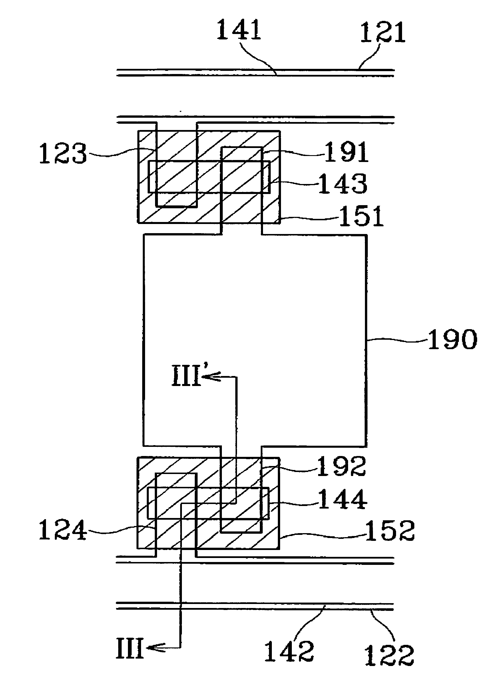
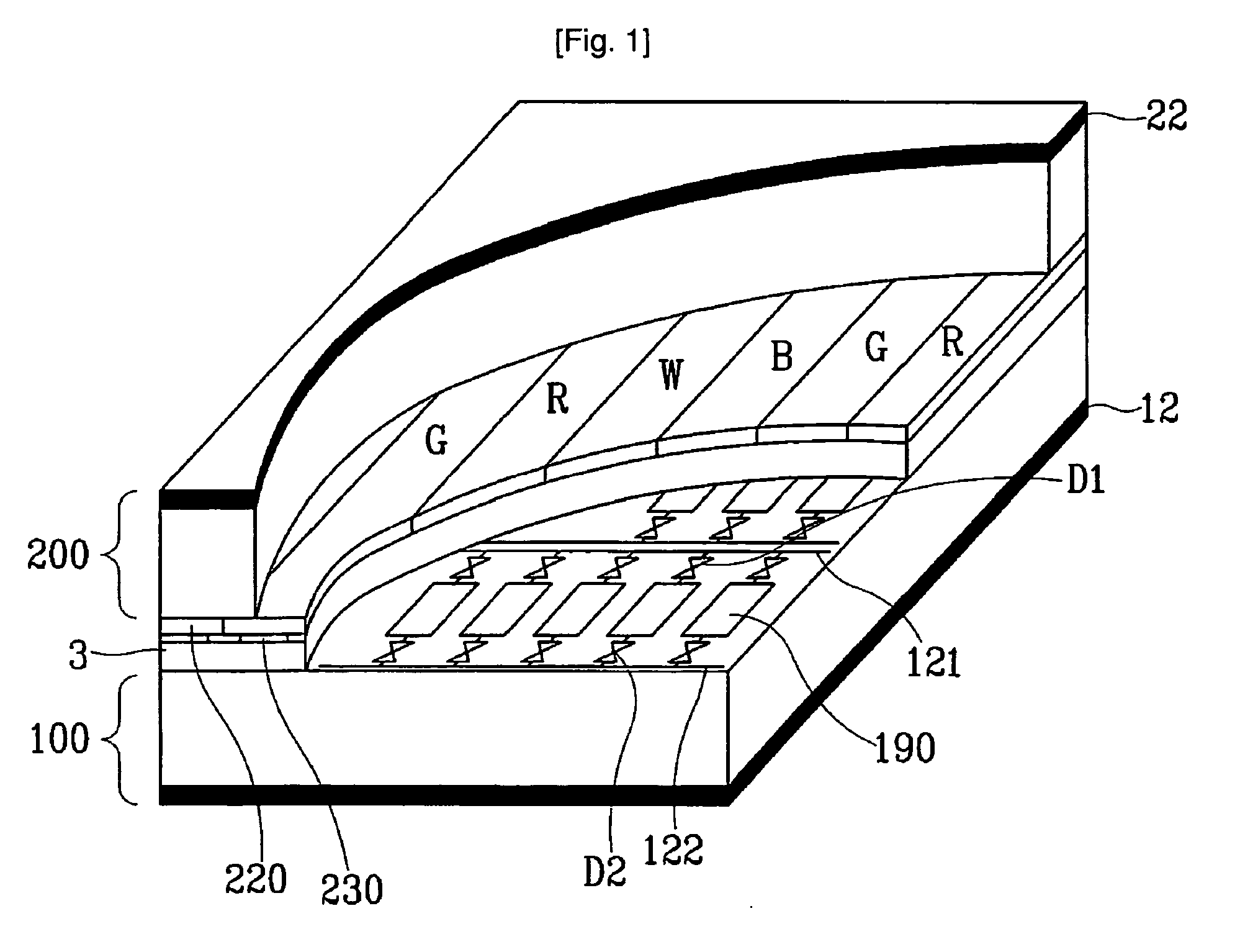
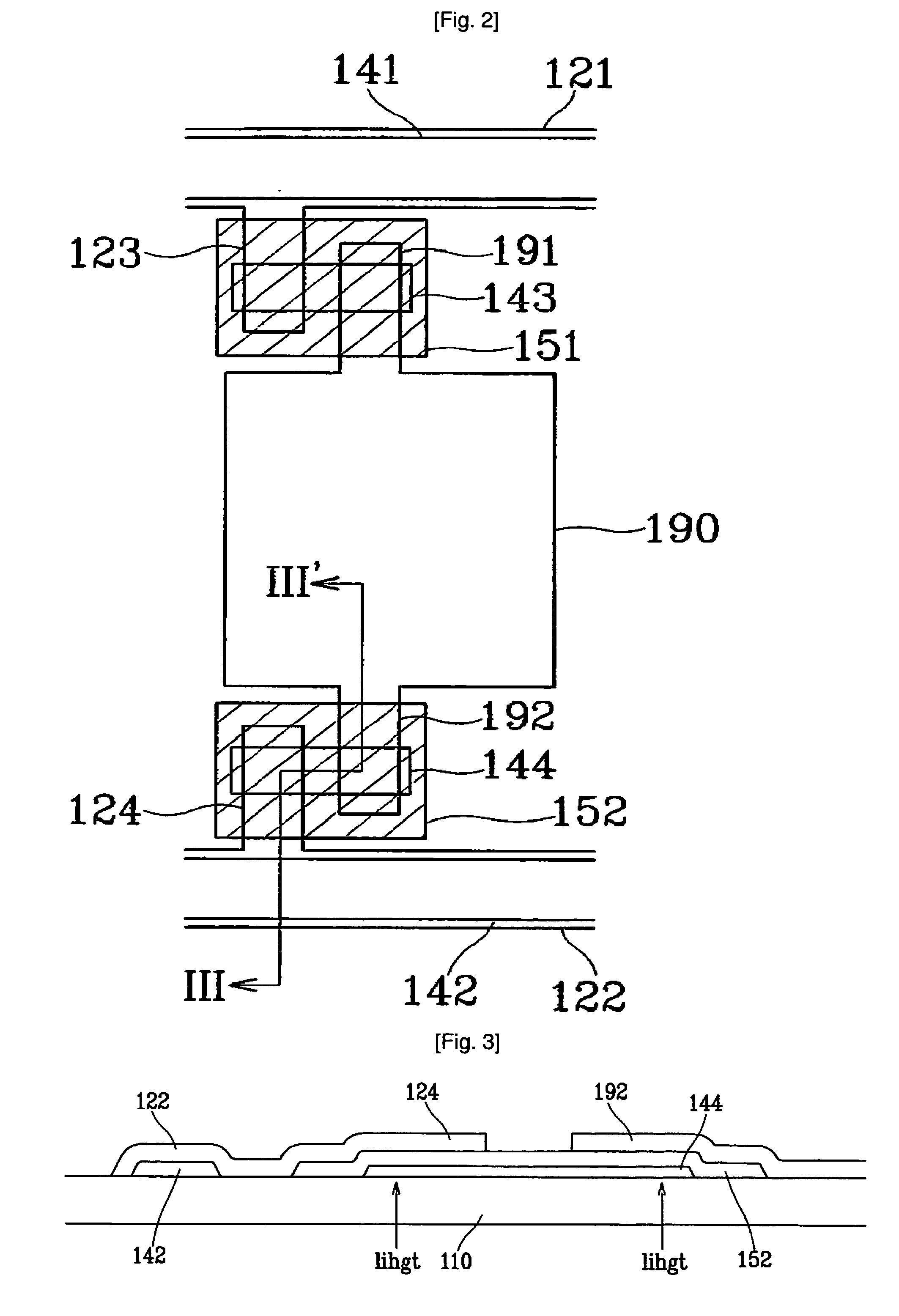
[0045]FIG. 1 is a perspective view of a liquid crystal display according to an embodiment of the present inve...


PUM


Abstract

A thin film diode array panel comprising: an insulating substrate (110); first and second redundant gate lines (141, 142) made of an opaque conductor and formed on the insulating substrate; first and second floating electrodes (143, 144) made of an opaque conductor, formed on the insulating substrate, and disposed between the first and second redundant gate lines (141, 142); an insulating layer (151, 152) formed on the first and second floating electrodes (143, 144); a first gate line (121) formed on the first redundant gate line (141) and including a first input electrode (123) overlapping the first floating electrode (143) where the insulating layer (151) is interposed between the first input electrode and the first floating electrode; a second gate line (122) formed on the second redundant gate line (142) and including a second input electrode (124) overlapping the second floating electrode (144) where the insulating layer (152) is interposed between the second input electrode (124) and the second floating electrode (144); and a pixel electrode (190) including a first contact electrode (191) overlapping the first floating electrode (143) where the insulating layer (151) is interposed between the first contact electrode (191) and the first floating electrode (143), a second contact electrode (192) overlapping the second floating electrode (144) where the insulating layer (152) is interposed between the second contact electrode (192) and the second floating electrode (144), and a main body is provided.

Description

TECHNICAL FIELD [0001] The present disclosure relates to thin film diode array panels using metal insulator metal (MIM) diodes as switching elements, and a manufacturing method of the same. In more detail, the present disclosure relates to thin film diode array panels of a dual select diode (DSD) type, and a liquid crystal display using the same. BACKGROUND ART [0002] A liquid crystal display (LCD) is one of the most widely used flat panel displays. An LCD includes two panels provided with field-generating electrodes, and a liquid crystal (LC) layer interposed therebetween. The LCD displays images by applying voltages to the field-generating electrodes to generate an electric field in the LC layer, which determines orientations of LC molecules in the LC layer to adjust polarization of incident light. [0003] An LCD may have switching elements to switch voltages of pixels arranged in a matrix form. An LCD can display various images since pixel voltages are individually switched. An LC...

Claims


Application Information

Patent Timeline
IPC IPC(8): G02F1/136G02F1/1343G02F1/1362G02F1/1365
CPCG02F1/13624G02F1/136286G02F1/1365G02F2001/13629G02F1/13629
Inventor SHIN, KYOUNG-JUCHAI, CHONG-CHULOH, JOON-HAKKIM, JIN-HONGHONG, JIN-SUNG
Owner SAMSUNG DISPLAY CO LTD
Why Eureka
Try Eureka